Advertisements
Online Mock Tests
Chapters
2: Physics and Mathematics
3: Rest and Motion: Kinematics
4: The Forces
5: Newton's Laws of Motion
6: Friction
7: Circular Motion
8: Work and Energy
9: Centre of Mass, Linear Momentum, Collision
10: Rotational Mechanics
11: Gravitation
12: Simple Harmonics Motion
13: Fluid Mechanics
14: Some Mechanical Properties of Matter
15: Wave Motion and Waves on a String
16: Sound Waves
17: Light Waves
18: Geometrical Optics
19: Optical Instruments
20: Dispersion and Spectra
21: Speed of Light
22: Photometry
23: Heat and Temperature
24: Kinetic Theory of Gases
25: Calorimetry
26: Laws of Thermodynamics
27: Specific Heat Capacities of Gases
28: Heat Transfer
29: Electric Field and Potential
30: Gauss’s Law
31: Capacitors
32: Electric Current in Conductors
33: Thermal and Chemical Effects of Current
34: Magnetic Field
35: Magnetic Field due to a Current
36: Permanent Magnets
37: Magnetic Properties of Matter
38: Electromagnetic Induction
39: Alternating Current
40: Electromagnetic Waves
41: Electric Current through Gases
42: Photoelectric Effect and Wave-Particle Duality
43: Bohr’s Model and Physics of Atom
44: X-rays
▶ 45: Semiconductors and Semiconductor Devices
46: The Nucleus
47: The Special Theory of Relativity
![HC Verma solutions for Concepts of Physics Volume 1 and 2 [English] chapter 45 - Semiconductors and Semiconductor Devices - Shaalaa.com](/images/concepts-of-physics-volume-1-and-2-english_6:9bad16cab2dd4ae1a1a6bac3add1eb27.jpg "HC Verma solutions for Concepts of Physics Volume 1 and 2 [English] chapter 45 - Semiconductors and Semiconductor Devices")
Advertisements
Solutions for Chapter 45: Semiconductors and Semiconductor Devices
Below listed, you can find solutions for Chapter 45 of CBSE, Karnataka Board PUC HC Verma for Concepts of Physics Volume 1 and 2 [English].
HC Verma solutions for Concepts of Physics Volume 1 and 2 [English] 45 Semiconductors and Semiconductor Devices Short Answers [Pages 416 - 417]
How many 1s energy states are present in one mole of sodium vapour? Are they all filled in normal conditions? How many 3s energy states are present in one mole of sodium vapour? Are they all filled in normal conditions?
There are energy bands in a solid. Do we have really continuous energy variation in a band ro do we have very closely spaced but still discrete energy levels?
The conduction band of a solid is partially filled at 0 K. Will it be a conductor, a semiconductor or an insulator?
In semiconductors, thermal collisions are responsible for taking a valence electron to the conduction band. Why does the number of conduction electrons not go on increasing with time as thermal collisions continuously take place?
When an electron goes from the valence band to the conduction band in silicon, its energy is increased by 1.1 eV. The average energy exchanged in a thermal collision is of the order of kT which is only 0.026 eV at room temperature. How is a thermal collision able to take some to the electrons from the valence band to the conduction band?
What is the resistance of an intrinsic semiconductor at 0 K?
We have valence electrons and conduction electrons in a semiconductor. Do we also have 'valence holes' and 'conduction holes'?
When a p-type impurity is doped in a semiconductor, a large number of holes are created, This does not make the semiconductor charged. But when holes diffuse from the p-side to the n-side in a p-n junction, the n-side gets positively charged. Explain.
The drift current in a reverse-biased p-n junction is increased in magnitude if the temperature of the junction is increased. Explain this on the basis of creation of hole-electron pairs.
An ideal diode should pass a current freely in one direction and should stop it completely in the opposite direction. Which is closer to ideal-vacuum diode or a p-njunction diode?
Consider an amplifier circuit using a transistor. The output power is several times greater than the input power. Where does the extra power come from?
HC Verma solutions for Concepts of Physics Volume 1 and 2 [English] 45 Semiconductors and Semiconductor Devices MCQ [Pages 417 - 418]
Electric conduction in a semiconductor takes place due to
electrons only
holes only
both electrons and holes
neither electrons nor holes.
An electric field is applied to a semiconductor. Let the number of charge carries be nand the average drift speed by v. If the temperature is increased,
both n and v will increase
n will increase but v will decrease
v will increase but n will decrease
both n and v will decrease.
Let np and ne be the number of holes and conduction electrons in an intrinsic semiconductor.
np > ne
np = ne
np < ne
np ≠ ne
Let np and ne be the numbers of holes and conduction electrons in an extrinsic semiconductor.
np > ne
np = ne
np < ne
np ≠ ne
A p-type semiconductor is
positively charged
negatively charged
uncharged
uncharged at O K but charged at higher temperatures.
When an impurity is doped into an intrinsic semiconductor, the conductivity of the semiconductor
increases
decreases
remains the same
become zero.
If the two ends of a p-n junction are joined by a wire,
there will not be a steady current in the circuit
there will be a steady current from the n-side to the p-side
there will a steady current from the p-side to the n-side
there may or may not be a current depending upon the resistance of the connecting wire
The drift current in a p-n junction is
from the n-side to the p-side
from the p-side to the n-side
from the p-side to the side if the junction is forward-biased and the opposite direction if it is reverse-biased
from the p-side to the n-side if the junction is forward-baised and in the opposite direction if it is reverse-biased.
The diffusion current in a p-n junction is
from the n-side ot the p-side
from the p-side to the n-side
from the n-side to the p-side if the junction is forward-biased and in the opposite direction if it is reverse-biased
from the p-side to the n-side if the junction is forward and in the opposite direction if it is reverse-biased.
Diffusion current in a p-n junction is greater than the drift current in magnitude
if the junction is forward-biased
if the junction is reverse-biased
if the junction is unbiased
in no case.
Two identical p-n junction may be connected in series with a battery in three ways. The potential difference across the two p-n junctions are equal in

circuit 1 and circuit 2
circuit 2 and circuit 3
circuit 3 and circuit 1
circuit 1 only.
Two identical capacitors A and B are charged to the same potential V and are connected in two circuits at t = 0 as shown in figure. The charges on the capacitors at a time t = CRare, respectively,
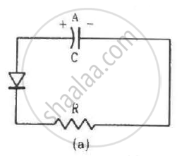
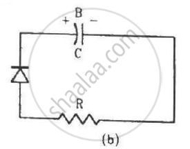
VC, VC
VC/e, VC
VC, VC/e
VC/e, VC/e.
A hole diffuses from the p-side to the n-side in a p-n junction. This means that
a bond is broken on the n-side and the electron freed from the bond jumps to the conduction band
a conduction electron on the p-side jumps to a broken bond to complete it
a bond is broken on the n-side and the electron freed from the bond jumps to a broken bond on the p-side to complete it
a bond is broken on the p-side and the electron freed from the bond jumps to a broken bond on the n-side to complete it.
In a transistor,
the emitter has the least concentration of impurity
the collector has the least concentration of impurity
the base has the least concentration of impurity
all the three regions have equal concentrations of impurity.
An incomplete sentence about transistors is given below:
The emitter−..... junction is __ and the collector−..... junction is __. The appropriate words for the dotted empty positions are, respectively,
'collector' and 'base'
'base' and 'emitter'
'collector' and 'emitter'
'base' and 'base'.
HC Verma solutions for Concepts of Physics Volume 1 and 2 [English] 45 Semiconductors and Semiconductor Devices MCQ [Page 418]
In a semiconductor,
(a) there are no free electrons at 0 K
(b) there are no free electrons at any temperature
(c) the number of free electrons increases with temperature
(d) the number of free electrons is less than that in a conductor.
In a p-n junction with open ends,
(a) there is no systematic motion of charge carries
(b) holes and conduction electrons systematically go from the p-side to n-side and from the n-side to p-side respectively
(c) there is no net charge transfer between the two sides
(d) there is a constant electric field near the junction.
In a p-n junction,
(a) new holes and conduction electrons are produced continuously throughout the material
(b) new holes and conduction electrons are produced continuously throughout the material except in the depletion region
(c) holes and conduction electrons recombine continuously throughout the material
(d) holes and conduction electrons recombine continuously throughout the material except in the depletion region.
The impurity atoms with which pure silicon may be doped to make it a p-type semiconductor are those of
(a) phosphorus
(b) boron
(c) antimony
(d) aluminium.
The electrical conductivity of pure germanium can be increased by
(a) increasing the temperature
(b) doping acceptor impurities
(c) doping donor impurities
(d) irradiating ultraviolet light on it.
A semiconducting device is connected in a series circuit with a battery and a resistance. A current is found to pass through the circuit. If the polarity of the battery is reversed, the current drops to almost zero. the device may be
(a) an intrinsic semiconductor
(b) a p-type semiconductor
(c) an n-type semiconductor
(d) a p-n junction
A semiconductor is doped with a donor impurity.
The hole concentration increases.
The hole concentration decreases.
The electron concentration increases.
The electron concentration decreases.
Let iE, iC and iB represent the emitter current, the collector current and the base current respectively in a transistor. Then
(a) iC is slightly smaller than iE
(b) iC is slightly greater than iE
(c) iB is much smaller than iE
(d) iB is much greater than iE.
In a normal operation of a transistor,
(a) the base−emitter junction is forward-baised
(b) the base−collector junction is forward-baised
(c) the base−emitter junction is reverse-baised
(d) the base−collector junction is reverse-baised.
An AND gate can be prepared by repetitive use of
(a) NOT gate
(b) OR gate
(c) NAND gate
(d) NOR gate.
HC Verma solutions for Concepts of Physics Volume 1 and 2 [English] 45 Semiconductors and Semiconductor Devices Exercises [Pages 419 - 421]
Calculate the number of states per cubic metre of sodium in 3s band. The density of sodium is 1013 kgm−3. How many of them are empty?
In a pure semiconductor, the number of conduction election 6 × 10¹⁹ per cubic metre. How many holes are there in a sample of size 1 cm × 1 mm?
Indium antimonide has a band gap of 0.23 eV between the valence and the conduction band. Find the temperature at which kT equals the band gap.
The band gap for silicon is 1.1 eV. (a) Find the ratio of the band gap to kT for silicon at room temperature 300 K. (b) At what temperature does this ratio become one tents of the value at 300 K? (Silicon will not retain its structure at these high temperatures.)
(Use Planck constant h = 4.14 × 10⁻¹⁵ eV-s, Boltzmann constant k = 8·62 × 10-5 eV/K.)
When a semiconducting material is doped with an impurity, new acceptor levels are created. In a particular thermal collision, a valence electron receives an energy equal to 2kT and just reaches one of the acceptor levels. Assuming that the energy of the electron was at the top edge of the valence band and that the temperature T is equal to 300 K, find the energy of the acceptor levels above the valence band.
The band gap between the valence and the conduction bands in zinc oxide (ZnO) is 3.2 eV. Suppose an electron in the conduction band combines with a hole in the valence band and the excess energy is released in the form of electromagnetic radiation. Find the maximum wavelength that can be emitted in this process.
Suppose the energy liberated in the recombination of a hole-electron pair is converted into electromagnetic radiation. If the maximum wavelength emitted is 820 nm, what is the band gap?
(Use Planck constant h = 4.14 × 10⁻¹⁵ eV-s, Boltzmann constant k = 8·62 × 10-5 eV/K.)
Find the maximum wavelength of electromagnetic radiation which can create a hole-electron pair in germanium. The band gap in germanium is 0.65 eV.
(Use Planck constant h = 4.14 × 10⁻¹⁵ eV-s, Boltzmann constant k = 8·62 × 10-5 eV/K.)
In a photo diode, the conductive increases when the material is exposed to light. It is found that the conductivity changes only if the wavelength is less than 620 nm. What is the band gap?
(Use Planck constant h = 4.14 × 10⁻¹⁵ eV-s, Boltzmann constant k = 8·62 × 10-5 eV/K.)
Let ΔE denote the energy gap between the valence band and the conduction band. The population of conduction electrons (and of the holes) is roughly proportional to e−ΔE/2kT. Find the ratio of the concentration of conduction electrons in diamond to the in silicon at room temperature 300 K. ΔE for silicon is 1.1 eV and for diamond is 6.1 eV. How many conduction electrons are likely to be in one cubic metre of diamond?
The conductivity of a pure semiconductor is roughly proportional to T3/2 e−ΔE/2kT where ΔE is the band gap. The band gap for germanium is 0.74 eV at 4 K and 0.67 eV at 300 K. By what factor does the conductivity of pure germanium increase as the temperature is raised from 4 K to 300 K?
Estimate the proportion of boron impurity which will increase the conductivity of a pure silicon sample by a factor of 100. Assume that each boron atom creates a hole and the concentration of holes in pure silicon at the same temperature is 7 × 10¹⁵ holes per cubic metre. Density of silicon 5 × 1028 atoms per cubic metre.
The product of the hole concentration and the conduction electron concentration turns out to be independent of the amount of any impurity doped. The concentration of conduction electrons in germanium is 6 × 10¹⁹ per cubic metref conduction electrons increases to 2 × 10²³ per cubic metre. Find the concentration of the holes in the doped germanium.. When some phosphorus impurity is doped into a germanium sample, the concentration o
The conductivity of an intrinsic semiconductor depends on temperature as σ = σ0e−ΔE/2kT, where σ0 is a constant. Find the temperature at which the conductivity of an intrinsic germanium semiconductor will be double of its value at T = 300 K. Assume that the gap for germanium is 0.650 eV and remains constant as the temperature is increased.
(Use Planck constant h = 4.14 × 10⁻¹⁵ eV-s, Boltzmann constant k = 8·62 × 10-5 eV/K.)
A semiconducting material has a band gap of 1 eV. Acceptor impurities are doped into it which create acceptor levels 1 meV above the valence band. Assume that the transition from one energy level to the other is almost forbidden if kT is less than 1/50 of the energy gap. Also if kT is more than twice the gap, the upper levels have maximum population. The temperature of the semiconductor is increased from 0 K. The concentration of the holes increases with temperature and after a certain temperature it becomes approximately constant. As the temperature is further increased, the hole concentration again starts increasing at a certain temperature. Find the order of the temperature range in which the hole concentration remains approximately constant.
(Use Planck constant h = 4.14 × 10⁻¹⁵ eV-s, Boltzmann constant k = 8·62 × 10-5 eV/K.)
In a p.n junction, the depletion region is 400 nm wide and an electric field of 5 × 10⁵ V m−1 exists in it. (a) Find the height of the potential barrier. (b) What should be the minimum kinetic energy of a conduction electron which can diffuse from the n-side to the p-side?
The potential barrier existing across an unbiased p-n junction is 0.2 volt. What minimum kinetic energy a hole should have to diffuse from the p-side to the n-side if (a) the junction is unbiased, (b) the junction is forward-biased at 0.1 volt and (c) the junction is reverse-biased at 0.1 volt?
In a p-n junction, a potential barrier of 250 meV exists across the junction. A hole with a kinetic energy of 300 meV approaches the junction. Find the kinetic energy of the hole when it crosses the junction if the hole approached the junction (a) from the p-side and (b) from the n-side.
When a p-n junction is reverse-biased, the current becomes almost constant at 25 µA. When it is forward-biased at 200 mV, a current of 75 µA is obtained. Find the magnitude of diffusion current when the diode is
(a) unbiased,
(b) reverse-biased at 200 mV and
(c) forward-biased at 200 mV.
The drift current in a p-n junction is 20.0 µA. Estimate the number of electrons crossing a cross section per second in the depletion region.
The current−voltage characteristic of an ideal p-n junction diode is given by \[i = i_0 ( e^{eV/KT} - 1)\] where, the drift current i0 equals 10 µA. Take the temperature T to be 300 K. (a) Find the voltage V0 for which \[e^{eV/kT} = 100 .\]One can neglect the term 1 for voltages greater than this value. (b) Find an expression for the dynamic resistance of the diode as a function of V for V > V0. (c) Find the voltage for which the dynamic resistance is 0.2 Ω.
(Use Planck constant h = 4.14 × 10⁻¹⁵ eV-s, Boltzmann constant k = 8·62 × 10-5 eV/K.)
Consider a p-n junction diode having the characteristic \[i - i_0 ( e^{eV/kT} - 1) \text{ where } i_0 = 20\mu A\] . The diode is operated at T = 300 K . (a) Find the current through the diode when a voltage of 300 mV is applied across it in forward bias. (b) At what voltage does the current double?
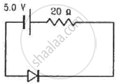
Calculate the current through the circuit and the potential difference across the diode shown in figure. The drift current for the diode is 20 µA.
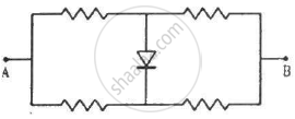
Each of the resistance shown in figure has a value of 20 Ω. Find the equivalent resistance between A and B. Does it depend on whether the point A or B is at higher potential?
Find the currents through the resistance in the circuits shown in figure.
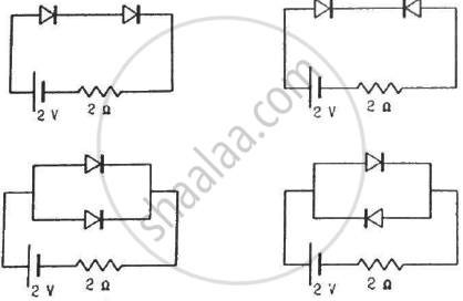
(Assume that the resistance of each diode is zero in forward bias and is infinity in reverse bias.)
What are the readings of the ammeters A1 and A2 shown in figure. Neglect the resistance of the meters.
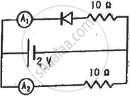
(Assume that the resistance of each diode is zero in forward bias and is infinity in reverse bias.)
Find the current through the battery in each of the circuits shown in figure.
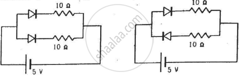
(Assume that the resistance of each diode is zero in forward bias and is infinity in reverse bias.)
Find the current through the resistance R in figure if (a) R = 12Ω (b) R = 48Ω.
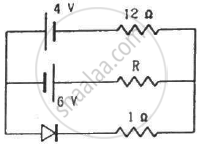
(Assume that the resistance of each diode is zero in forward bias and is infinity in reverse bias.)
Draw the current-voltage characteristics for the device show in figure between the terminals A and B.
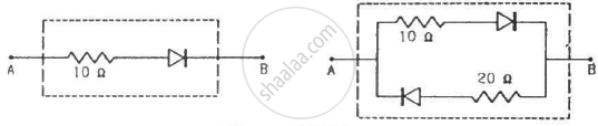
(Assume that the resistance of each diode is zero in forward bias and is infinity in reverse bias.)
Find the equivalent resistance of the network shown in figure between the points A and B.
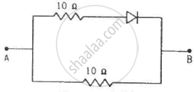
(Assume that the resistance of each diode is zero in forward bias and is infinity in reverse bias.)
When the base current in a transistor is changed from 30µA to 80µA, the collector current is changed from 1.0 mA to 3.5 mA. Find the current gain β.
A load resistor of 2kΩ is connected in the collector branch of an amplifier circuit using a transistor in common-emitter mode. The current gain β = 50. The input resistance of the transistor is 0.50 kΩ. If the input current is changed by 50µA. (a) by what amount does the output voltage change, (b) by what amount does the input voltage change and (c) what is the power gain?
Let \[X = A \overline{ BC} + B\overline{ CA} + C\overline{AB } .\] Evaluate X for A = 1, B = 0, C = 1.
Let \[X = A \overline{ BC} + B\overline{ CA} + C\overline{AB } .\] Evaluate X for A = B = C = 1.
Let \[X = A \overline{ BC} + B\overline{ CA} + C\overline{AB } .\] Evaluate X for A = B = C = 0.
Design a logical circuit using AND, OR and NOT gates to evaluate \[A \overline { BC } + B \overline{ CA }\] .
Show that \[AB + \overline {AB }\] is always 1.
Solutions for 45: Semiconductors and Semiconductor Devices
HC Verma solutions for Concepts of Physics Volume 1 and 2 [English] chapter 45 - Semiconductors and Semiconductor Devices
Shaalaa.com has the CBSE, Karnataka Board PUC Mathematics Concepts of Physics Volume 1 and 2 [English] CBSE, Karnataka Board PUC solutions in a manner that help students grasp basic concepts better and faster. The detailed, step-by-step solutions will help you understand the concepts better and clarify any confusion. HC Verma solutions for Mathematics Concepts of Physics Volume 1 and 2 [English] CBSE, Karnataka Board PUC 45 (Semiconductors and Semiconductor Devices) include all questions with answers and detailed explanations. This will clear students' doubts about questions and improve their application skills while preparing for board exams.
Further, we at Shaalaa.com provide such solutions so students can prepare for written exams. HC Verma textbook solutions can be a core help for self-study and provide excellent self-help guidance for students.
Concepts covered in Concepts of Physics Volume 1 and 2 [English] chapter 45 Semiconductors and Semiconductor Devices are Concept of Semiconductor Electronics, Diode or p-n Junction, Classification of Metals, Conductors and Semiconductors, Intrinsic Semiconductor, Extrinsic Semiconductor, Semiconductor Diode, n-type Semiconductor, p-type Semiconductor, Overview: Semiconductor Electronics, Application of Junction Diode as a Rectifier.
Using HC Verma Concepts of Physics Volume 1 and 2 [English] solutions Semiconductors and Semiconductor Devices exercise by students is an easy way to prepare for the exams, as they involve solutions arranged chapter-wise and also page-wise. The questions involved in HC Verma Solutions are essential questions that can be asked in the final exam. Maximum CBSE, Karnataka Board PUC Concepts of Physics Volume 1 and 2 [English] students prefer HC Verma Textbook Solutions to score more in exams.
Get the free view of Chapter 45, Semiconductors and Semiconductor Devices Concepts of Physics Volume 1 and 2 [English] additional questions for Mathematics Concepts of Physics Volume 1 and 2 [English] CBSE, Karnataka Board PUC, and you can use Shaalaa.com to keep it handy for your exam preparation.
