Advertisements
Advertisements
Question
Draw the current-voltage characteristics for the device show in figure between the terminals A and B.

(Assume that the resistance of each diode is zero in forward bias and is infinity in reverse bias.)
Advertisements
Solution
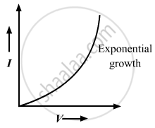
(a) If a battery is connected between terminals A and B, with positive terminal connected to point A and negative terminal connected to point B, then the diode will get forward biassed by the applied voltage. So, the current voltage graph for this circuit will be the same as that of the characteristic curves of a forward-biassed diode.
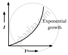
(b) If a battery is connected between terminals A and B, with positive terminal connected to point A and negative terminal connected to point B, then the upper diode will get forward biassed and the lower diode will get reverse biassed by the applied voltage. So, this lower branch can be replaced by an open circuit; hence, the current flow through this branch will be zero. The current flows only through the upper diode, so the circuit on simplification will become identical to the circuit in part (a). Hence, the current voltage graph for this circuit will be the same as that of the characteristic curves of a forward-biassed diode.
APPEARS IN
RELATED QUESTIONS
In a p-n junction diode, the current I can be expressed as
I = `"I"_0 exp ("eV"/(2"k"_"BT") - 1)`
where I0 is called the reverse saturation current, V is the voltage across the diode and is positive for forward bias and negative for reverse bias, and I is the current through the diode, kBis the Boltzmann constant (8.6×10⁻⁵ eV/K) and T is the absolute temperature. If for a given diode I0 = 5 × 10⁻¹² A and T = 300 K, then
(a) What will be the forward current at a forward voltage of 0.6 V?
(b) What will be the increase in the current if the voltage across the diode is increased to 0.7 V?
(c) What is the dynamic resistance?
(d) What will be the current if reverse bias voltage changes from 1 V to 2 V?
Explain, with the help of a circuit diagram, the working of a photo-diode. Write briefly how it is used to detect the optical signals.
Mention the important considerations required while fabricating a p-n junction diode to be used as a Light Emitting Diode (LED). What should be the order of band gap of an LED if it is required to emit light in the visible range?
Draw a circuit diagram to study the input and output characteristics of an n-p-n transistor in its common emitter configuration. Draw the typical input and output characteristics.
Explain, with the help of a circuit diagram, the working of n-p-n transistor as a common emitter amplifier.
When a p-type impurity is doped in a semiconductor, a large number of holes are created, This does not make the semiconductor charged. But when holes diffuse from the p-side to the n-side in a p-n junction, the n-side gets positively charged. Explain.
The drift current in a reverse-biased p-n junction is increased in magnitude if the temperature of the junction is increased. Explain this on the basis of creation of hole-electron pairs.
When a p-n junction is reverse-biased, the current becomes almost constant at 25 µA. When it is forward-biased at 200 mV, a current of 75 µA is obtained. Find the magnitude of diffusion current when the diode is
(a) unbiased,
(b) reverse-biased at 200 mV and
(c) forward-biased at 200 mV.
The drift current in a p-n junction is 20.0 µA. Estimate the number of electrons crossing a cross section per second in the depletion region.
The current−voltage characteristic of an ideal p-n junction diode is given by \[i = i_0 ( e^{eV/KT} - 1)\] where, the drift current i0 equals 10 µA. Take the temperature T to be 300 K. (a) Find the voltage V0 for which \[e^{eV/kT} = 100 .\]One can neglect the term 1 for voltages greater than this value. (b) Find an expression for the dynamic resistance of the diode as a function of V for V > V0. (c) Find the voltage for which the dynamic resistance is 0.2 Ω.
(Use Planck constant h = 4.14 × 10⁻¹⁵ eV-s, Boltzmann constant k = 8·62 × 10-5 eV/K.)
Consider a p-n junction diode having the characteristic \[i - i_0 ( e^{eV/kT} - 1) \text{ where } i_0 = 20\mu A\] . The diode is operated at T = 300 K . (a) Find the current through the diode when a voltage of 300 mV is applied across it in forward bias. (b) At what voltage does the current double?
Each of the resistance shown in figure has a value of 20 Ω. Find the equivalent resistance between A and B. Does it depend on whether the point A or B is at higher potential?

Find the currents through the resistance in the circuits shown in figure.

(Assume that the resistance of each diode is zero in forward bias and is infinity in reverse bias.)
Find the equivalent resistance of the network shown in figure between the points A and B.

(Assume that the resistance of each diode is zero in forward bias and is infinity in reverse bias.)
An AC source is connected to a diode and a resistor in series. Is the current thorough the resistor AC or DC?
A diode, a resistor and a 50 Hz AC source are connected in series. The number of current pulses per second through the resistor is __________ .
In a semiconductor diode, the barrier potential offers opposition to only ______.
During the formation of a p-n junction ______.
In p-n junction diode ______.
