Advertisements
Advertisements
प्रश्न
Draw the current-voltage characteristics for the device show in figure between the terminals A and B.

(Assume that the resistance of each diode is zero in forward bias and is infinity in reverse bias.)
Advertisements
उत्तर
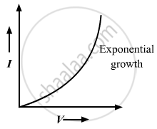
(a) If a battery is connected between terminals A and B, with positive terminal connected to point A and negative terminal connected to point B, then the diode will get forward biassed by the applied voltage. So, the current voltage graph for this circuit will be the same as that of the characteristic curves of a forward-biassed diode.
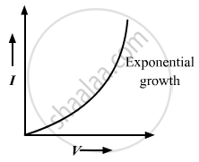
(b) If a battery is connected between terminals A and B, with positive terminal connected to point A and negative terminal connected to point B, then the upper diode will get forward biassed and the lower diode will get reverse biassed by the applied voltage. So, this lower branch can be replaced by an open circuit; hence, the current flow through this branch will be zero. The current flows only through the upper diode, so the circuit on simplification will become identical to the circuit in part (a). Hence, the current voltage graph for this circuit will be the same as that of the characteristic curves of a forward-biassed diode.
APPEARS IN
संबंधित प्रश्न
Write the two processes that take place in the formation of a p-n junction.
A student wants to use two p-n junction diodes to convert alternating current into direct current. Draw the labelled circuit diagram she would use and explain how it works.
Draw a circuit diagram to study the input and output characteristics of an n-p-n transistor in its common emitter configuration. Draw the typical input and output characteristics.
Explain, with the help of a circuit diagram, the working of n-p-n transistor as a common emitter amplifier.
A hole diffuses from the p-side to the n-side in a p-n junction. This means that
The potential barrier existing across an unbiased p-n junction is 0.2 volt. What minimum kinetic energy a hole should have to diffuse from the p-side to the n-side if (a) the junction is unbiased, (b) the junction is forward-biased at 0.1 volt and (c) the junction is reverse-biased at 0.1 volt?
What are the readings of the ammeters A1 and A2 shown in figure. Neglect the resistance of the meters.

(Assume that the resistance of each diode is zero in forward bias and is infinity in reverse bias.)
Find the current through the battery in each of the circuits shown in figure.

(Assume that the resistance of each diode is zero in forward bias and is infinity in reverse bias.)
Find the equivalent resistance of the network shown in figure between the points A and B.

(Assume that the resistance of each diode is zero in forward bias and is infinity in reverse bias.)
When the base current in a transistor is changed from 30µA to 80µA, the collector current is changed from 1.0 mA to 3.5 mA. Find the current gain β.
A load resistor of 2kΩ is connected in the collector branch of an amplifier circuit using a transistor in common-emitter mode. The current gain β = 50. The input resistance of the transistor is 0.50 kΩ. If the input current is changed by 50µA. (a) by what amount does the output voltage change, (b) by what amount does the input voltage change and (c) what is the power gain?
A diode, a resistor and a 50 Hz AC source are connected in series. The number of current pulses per second through the resistor is __________ .
In a semiconductor diode, the barrier potential offers opposition to only ______.
p-n junction diode is formed
During the formation of a p-n junction ______.
Diode and resistance are connected as shown in figure. Out of the following statements which one is TRUE?

In p-n junction diode ______.
