Advertisements
Advertisements
प्रश्न
Explain briefly with the help of necessary diagrams, the reverse biasing of a p-n junction diode. Also draw characteristic curves.
Advertisements
उत्तर
p-n junction diode under reverse bias
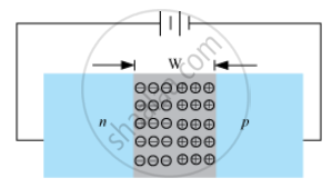
Positive terminal of battery is connected to n-side and negative terminal to p-side.
Reverse bias supports the potential barrier. Therefore, the barrier height increases and the width of depletion region also increases.
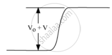
Effective barrier height under reverse bias is (V0 + V).
No conduction across the junction due to majority carriers; few minority carriers cross the junction after being accelerated by high reverse bias voltage
This constitutes a current that flows in opposite direction − celled reverse current.
APPEARS IN
संबंधित प्रश्न
Write the two processes that take place in the formation of a p-n junction.
When a p-type impurity is doped in a semiconductor, a large number of holes are created, This does not make the semiconductor charged. But when holes diffuse from the p-side to the n-side in a p-n junction, the n-side gets positively charged. Explain.
The diffusion current in a p-n junction is
The drift current in a p-n junction is 20.0 µA. Estimate the number of electrons crossing a cross section per second in the depletion region.
The current−voltage characteristic of an ideal p-n junction diode is given by \[i = i_0 ( e^{eV/KT} - 1)\] where, the drift current i0 equals 10 µA. Take the temperature T to be 300 K. (a) Find the voltage V0 for which \[e^{eV/kT} = 100 .\]One can neglect the term 1 for voltages greater than this value. (b) Find an expression for the dynamic resistance of the diode as a function of V for V > V0. (c) Find the voltage for which the dynamic resistance is 0.2 Ω.
(Use Planck constant h = 4.14 × 10⁻¹⁵ eV-s, Boltzmann constant k = 8·62 × 10-5 eV/K.)
A load resistor of 2kΩ is connected in the collector branch of an amplifier circuit using a transistor in common-emitter mode. The current gain β = 50. The input resistance of the transistor is 0.50 kΩ. If the input current is changed by 50µA. (a) by what amount does the output voltage change, (b) by what amount does the input voltage change and (c) what is the power gain?
Choose the correct option.
Current through a reverse-biased p-n junction increases abruptly at:
The depletion layer in the p-n junction diode is caused by ______.
Zener breakdown occurs in a p-n junction having p and n both:
During the formation of a p-n junction ______.
