Advertisements
Advertisements
प्रश्न
How is a zener diode fabricated so as to make it a special purpose diode? Draw I-V characteristics of zener diode and explain the significance of breakdown voltage.
Explain briefly, with the help of a circuit diagram, how a p-n junction diode works as a half wave rectifier.
Advertisements
उत्तर
Zener is fabricated such that both the p-type and the n-type are highly doped. This makes the depletion region thin. When an electric field is applied, a high electric field appears across the thin depletion region. When the electric field becomes very high, it knocks off electrons from the host atoms to create a large number of electrons. This results in a large value of current inside the circuit.
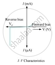
Zener has a sharp breakdown voltage and this property of zener is used for voltage regulation.
An ac current has a positive half cycle and a negative half cycle. A pn junction allows current to pass only in one direction and that is when it is forward biased.
When a positive half-cycle occurs, the p-side has a lower potential. Therefore, the diode is now forward biased and therefore conducts and this positive cycle is available for the load.
When a negative half cycle occurs, the n-side has a higher potential than the p-side. Hence, the diode is now reverse biased and thus, does not conduct. As a result, this positive half cycle also does not conduct. Therefore, it does not appear at the load and is cut-off.
We obtain a waveform, which has only positive half cycles and therefore it is called half-wave rectifier.
APPEARS IN
संबंधित प्रश्न
In an unbiased p-n junction, holes diffuse from the p-region to n-region because ______.
If the two ends of a p-n junction are joined by a wire,
In a p-n junction with open ends,
(a) there is no systematic motion of charge carries
(b) holes and conduction electrons systematically go from the p-side to n-side and from the n-side to p-side respectively
(c) there is no net charge transfer between the two sides
(d) there is a constant electric field near the junction.
A semiconducting device is connected in a series circuit with a battery and a resistance. A current is found to pass through the circuit. If the polarity of the battery is reversed, the current drops to almost zero. the device may be
(a) an intrinsic semiconductor
(b) a p-type semiconductor
(c) an n-type semiconductor
(d) a p-n junction
When a p-n junction is reverse-biased, the current becomes almost constant at 25 µA. When it is forward-biased at 200 mV, a current of 75 µA is obtained. Find the magnitude of diffusion current when the diode is
(a) unbiased,
(b) reverse-biased at 200 mV and
(c) forward-biased at 200 mV.
Consider a p-n junction diode having the characteristic \[i - i_0 ( e^{eV/kT} - 1) \text{ where } i_0 = 20\mu A\] . The diode is operated at T = 300 K . (a) Find the current through the diode when a voltage of 300 mV is applied across it in forward bias. (b) At what voltage does the current double?
Find the currents through the resistance in the circuits shown in figure.

(Assume that the resistance of each diode is zero in forward bias and is infinity in reverse bias.)
When the base current in a transistor is changed from 30µA to 80µA, the collector current is changed from 1.0 mA to 3.5 mA. Find the current gain β.
If in a p-n junction diode, a square input signal of 10 V is applied as shown Then the output signal across RL will be ______

The formation of the depletion region in a p-n junction diode is due to ______.
