Advertisements
Advertisements
प्रश्न
Explain, with the help of a circuit diagram, the working of a photo-diode. Write briefly how it is used to detect the optical signals.
Advertisements
उत्तर
Working of photo diode:
A junction diode made from light sensitive semi-conductor is called a photodiode.

A photodiode is an electrical device used to detect and convert light into an energy signal through the use of a photo detector. It is a pn-junction whose function is controlled by the light allowed to fall on it. Suppose, the wavelength is such that the energy of a photon, hc/λ, is sufficient to break a valance bond. When such light falls on the junction, new hole-electron pairs are created. The number of charge carriers increases and hence the conductivity of the junction increases. If the junction is connected in some circuit, the current in the circuit is controlled by the intensity of the incident light.
APPEARS IN
संबंधित प्रश्न
In an unbiased p-n junction, holes diffuse from the p-region to n-region because ______.
Write the two processes that take place in the formation of a p-n junction.
A zener diode is fabricated by heavily doping both p- and n- sides of the junction. Explain, why?
Explain briefly with the help of necessary diagrams, the forward biasing of a p-n junction diode. Also draw characteristic curves.
A hole diffuses from the p-side to the n-side in a p-n junction. This means that
Consider a p-n junction diode having the characteristic \[i - i_0 ( e^{eV/kT} - 1) \text{ where } i_0 = 20\mu A\] . The diode is operated at T = 300 K . (a) Find the current through the diode when a voltage of 300 mV is applied across it in forward bias. (b) At what voltage does the current double?
Draw the current-voltage characteristics for the device show in figure between the terminals A and B.
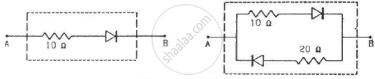
(Assume that the resistance of each diode is zero in forward bias and is infinity in reverse bias.)
Answer in detail.
Discuss the effect of external voltage on the width of depletion region of a p-n junction.
Zener breakdown occurs in a p-n junction having p and n both:
What is the net current in zero bias when diffusion and drift currents balance?
