Advertisements
Advertisements
प्रश्न
Consider a p-n junction diode having the characteristic \[i - i_0 ( e^{eV/kT} - 1) \text{ where } i_0 = 20\mu A\] . The diode is operated at T = 300 K . (a) Find the current through the diode when a voltage of 300 mV is applied across it in forward bias. (b) At what voltage does the current double?
Advertisements
उत्तर
(a) Given:-
Drift current, i0 = 20 × 10−6 A
Temperature, T = 300 K
Applied voltage, V = 300 mV
The variation in the current with respect to the voltage is given by
\[i = i_0 \left( e^\frac{eV}{KT} - 1 \right)\]
\[ \Rightarrow i = 20 \times {10}^{- 6} \left( e^\frac{0 . 3}{8 . 62 \times 300 \times {10}^{- 5}} - 1 \right)\]
\[ \Rightarrow i = 20 \times {10}^{- 5} \left( e^\frac{100}{8 . 61} - 1 \right)\]
\[ \Rightarrow i = 2 . 18 A \approx 2 \] A
(b) We need to find the voltage at which the current doubles so that the new value of the current becomes 4 A.
\[\Rightarrow 4 = 20 \times {10}^{- 6} \left( e^\frac{eV}{8 . 62 \times 3 \times {10}^{- 3}} - 1 \right)\]
\[ \Rightarrow e^\frac{V \times {10}^3}{8 . 62 \times 3} - 1 = \frac{4 \times {10}^6}{20}\]
\[ \Rightarrow e^\frac{V \times {10}^3}{8 . 62 \times 3} = 200001\]
\[ \Rightarrow \frac{V \times {10}^3}{8 . 62 \times 3} = 12 . 2060\]
\[ \Rightarrow V = \frac{12 . 206 \times 8 . 63 \times 3}{{10}^3}\]
\[ \Rightarrow V = 318 \] mV
APPEARS IN
संबंधित प्रश्न
When a p-type impurity is doped in a semiconductor, a large number of holes are created, This does not make the semiconductor charged. But when holes diffuse from the p-side to the n-side in a p-n junction, the n-side gets positively charged. Explain.
A hole diffuses from the p-side to the n-side in a p-n junction. This means that
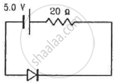
Calculate the current through the circuit and the potential difference across the diode shown in figure. The drift current for the diode is 20 µA.
What are the readings of the ammeters A1 and A2 shown in figure. Neglect the resistance of the meters.
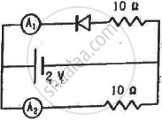
(Assume that the resistance of each diode is zero in forward bias and is infinity in reverse bias.)
Find the equivalent resistance of the network shown in figure between the points A and B.
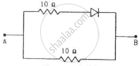
(Assume that the resistance of each diode is zero in forward bias and is infinity in reverse bias.)
A diode, a resistor and a 50 Hz AC source are connected in series. The number of current pulses per second through the resistor is __________ .
Answer in detail.
Discuss the effect of external voltage on the width of depletion region of a p-n junction.
If in a p-n junction diode, a square input signal of 10 V is applied as shown Then the output signal across RL will be ______

The depletion layer in the p-n junction diode is caused by ______.
p-n junction diode is formed
For an ideal diode, in forward and reverse biased condition the resistance is respectively ______.
What is a p-n junction diode?
Which process moves charge carriers from a higher concentration to a lower concentration?
When p-type and n-type regions are formed in a single crystal, which carriers initially diffuse from each side?
Why does microscopic roughness prevent a proper crystal lattice from forming between separate p-type and n-type slabs?
What role do diodes perform in electronic switching?
In which circuits are diodes used for signal detection?
What is the net current in zero bias when diffusion and drift currents balance?
