Advertisements
Advertisements
प्रश्न
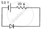
Calculate the current through the circuit and the potential difference across the diode shown in figure. The drift current for the diode is 20 µA.
Advertisements
उत्तर
(a) From the circuit diagram, it can be said that the diode is reverse biassed, with applied voltage of 5.0 V.
Under reverse bias condition,
Current in the circuit = Drift current
So, the current in the circuit is 20 µA.
(b) Voltage across the diode will be equal to the voltage of the battery minus the voltage drop across the 20 ohm resistor.
\[\Rightarrow V = 5 - iR\]
\[ \Rightarrow V = 5 - (20 \times 20 \times {10}^{- 6} )\]
\[ \Rightarrow V = 5 - (4 \times {10}^{- 4} )\]
\[ \Rightarrow V = {10}^{- 4} (50000 - 4)\]
\[ \Rightarrow V = 49996 \times {10}^{- 4} \]
\[ \Rightarrow V = 4 . 9996 V \cong 5\] V
APPEARS IN
संबंधित प्रश्न
Explain briefly with the help of necessary diagrams, the reverse biasing of a p-n junction diode. Also draw characteristic curves.
Mention the important considerations required while fabricating a p-n junction diode to be used as a Light Emitting Diode (LED). What should be the order of band gap of an LED if it is required to emit light in the visible range?
Draw a circuit diagram to study the input and output characteristics of an n-p-n transistor in its common emitter configuration. Draw the typical input and output characteristics.
Explain, with the help of a circuit diagram, the working of n-p-n transistor as a common emitter amplifier.
When a p-type impurity is doped in a semiconductor, a large number of holes are created, This does not make the semiconductor charged. But when holes diffuse from the p-side to the n-side in a p-n junction, the n-side gets positively charged. Explain.
In a p-n junction with open ends,
(a) there is no systematic motion of charge carries
(b) holes and conduction electrons systematically go from the p-side to n-side and from the n-side to p-side respectively
(c) there is no net charge transfer between the two sides
(d) there is a constant electric field near the junction.
In a p-n junction,
(a) new holes and conduction electrons are produced continuously throughout the material
(b) new holes and conduction electrons are produced continuously throughout the material except in the depletion region
(c) holes and conduction electrons recombine continuously throughout the material
(d) holes and conduction electrons recombine continuously throughout the material except in the depletion region.
In a p.n junction, the depletion region is 400 nm wide and an electric field of 5 × 10⁵ V m−1 exists in it. (a) Find the height of the potential barrier. (b) What should be the minimum kinetic energy of a conduction electron which can diffuse from the n-side to the p-side?
When a p-n junction is reverse-biased, the current becomes almost constant at 25 µA. When it is forward-biased at 200 mV, a current of 75 µA is obtained. Find the magnitude of diffusion current when the diode is
(a) unbiased,
(b) reverse-biased at 200 mV and
(c) forward-biased at 200 mV.
Find the current through the resistance R in figure if (a) R = 12Ω (b) R = 48Ω.
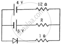
(Assume that the resistance of each diode is zero in forward bias and is infinity in reverse bias.)
A diode, a resistor and a 50 Hz AC source are connected in series. The number of current pulses per second through the resistor is __________ .
Zener breakdown occurs in a p-n junction having p and n both:
During the formation of a p-n junction ______.
What is drift?
Why does microscopic roughness prevent a proper crystal lattice from forming between separate p-type and n-type slabs?
What is the use of diodes in power supplies and chargers?
What is the net current in zero bias when diffusion and drift currents balance?
What is the approximate knee voltage for germanium?
Which formula gives the dynamic resistance of a diode?
