Advertisements
Advertisements
प्रश्न
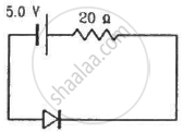
Calculate the current through the circuit and the potential difference across the diode shown in figure. The drift current for the diode is 20 µA.
Advertisements
उत्तर
(a) From the circuit diagram, it can be said that the diode is reverse biassed, with applied voltage of 5.0 V.
Under reverse bias condition,
Current in the circuit = Drift current
So, the current in the circuit is 20 µA.
(b) Voltage across the diode will be equal to the voltage of the battery minus the voltage drop across the 20 ohm resistor.
\[\Rightarrow V = 5 - iR\]
\[ \Rightarrow V = 5 - (20 \times 20 \times {10}^{- 6} )\]
\[ \Rightarrow V = 5 - (4 \times {10}^{- 4} )\]
\[ \Rightarrow V = {10}^{- 4} (50000 - 4)\]
\[ \Rightarrow V = 49996 \times {10}^{- 4} \]
\[ \Rightarrow V = 4 . 9996 V \cong 5\] V
APPEARS IN
संबंधित प्रश्न
In an unbiased p-n junction, holes diffuse from the p-region to n-region because ______.
A zener diode is fabricated by heavily doping both p- and n- sides of the junction. Explain, why?
Explain briefly with the help of necessary diagrams, the forward biasing of a p-n junction diode. Also draw characteristic curves.
Mention the important considerations required while fabricating a p-n junction diode to be used as a Light Emitting Diode (LED). What should be the order of band gap of an LED if it is required to emit light in the visible range?
Explain, with the help of a circuit diagram, the working of n-p-n transistor as a common emitter amplifier.
The drift current in a p-n junction is
The diffusion current in a p-n junction is
Find the current through the resistance R in figure if (a) R = 12Ω (b) R = 48Ω.
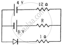
(Assume that the resistance of each diode is zero in forward bias and is infinity in reverse bias.)
Find the equivalent resistance of the network shown in figure between the points A and B.
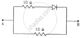
(Assume that the resistance of each diode is zero in forward bias and is infinity in reverse bias.)
A load resistor of 2kΩ is connected in the collector branch of an amplifier circuit using a transistor in common-emitter mode. The current gain β = 50. The input resistance of the transistor is 0.50 kΩ. If the input current is changed by 50µA. (a) by what amount does the output voltage change, (b) by what amount does the input voltage change and (c) what is the power gain?
An AC source is connected to a diode and a resistor in series. Is the current thorough the resistor AC or DC?
Choose the correct option.
Current through a reverse-biased p-n junction increases abruptly at:
Answer in detail.
Discuss the effect of external voltage on the width of depletion region of a p-n junction.
In a semiconductor diode, the barrier potential offers opposition to only ______.
Zener breakdown occurs in a p-n junction having p and n both:
Which process moves charge carriers from a higher concentration to a lower concentration?
In which direction is the electric field established by the fixed ions?
What is the approximate knee voltage for silicon?
