Advertisements
Advertisements
प्रश्न
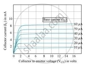
Draw a circuit diagram to study the input and output characteristics of an n-p-n transistor in its common emitter configuration. Draw the typical input and output characteristics.
Advertisements
उत्तर


APPEARS IN
संबंधित प्रश्न
Mention the important considerations required while fabricating a p-n junction diode to be used as a Light Emitting Diode (LED). What should be the order of band gap of an LED if it is required to emit light in the visible range?
Explain, with the help of a circuit diagram, the working of n-p-n transistor as a common emitter amplifier.
If the two ends of a p-n junction are joined by a wire,
The diffusion current in a p-n junction is
In a p-n junction,
(a) new holes and conduction electrons are produced continuously throughout the material
(b) new holes and conduction electrons are produced continuously throughout the material except in the depletion region
(c) holes and conduction electrons recombine continuously throughout the material
(d) holes and conduction electrons recombine continuously throughout the material except in the depletion region.
Find the current through the resistance R in figure if (a) R = 12Ω (b) R = 48Ω.

(Assume that the resistance of each diode is zero in forward bias and is infinity in reverse bias.)
Draw the current-voltage characteristics for the device show in figure between the terminals A and B.

(Assume that the resistance of each diode is zero in forward bias and is infinity in reverse bias.)
If in a p-n junction diode, a square input signal of 10 V is applied as shown Then the output signal across RL will be ______

p-n junction diode is formed
The formation of the depletion region in a p-n junction diode is due to ______.
