Topics
Electrostatics
Electric Charges and Fields
- Electric Charge
- Conductors and Insulators
- Properties of Electric Charge
- Coulomb’s Law
- Forces between Multiple Charges
- Electric Field
- Electric Field Due to a System of Charges
- Physical Significance of Electric Field
- Electric Field Lines
- Electric Flux
- Electric Dipole
- Dipole in a Uniform External Field
- Continuous Charge Distribution
- Gauss’s Law
- Application of Gauss' Law
Current Electricity
Electrostatic Potential and Capacitance
- Electric Potential and Potential Energy
- Electrostatic Potential
- Electric Potential Due to a Point Charge
- Potential Due to an Electric Dipole
- Potential due to a System of Charges
- Equipotential Surfaces
- Relation Between Electric Field and Electrostatic Potential
- Potential Energy of a System of Charges
- Potential Energy of a Single Charge
- Potential Energy of a System of Two Charges in an External Field
- Potential Energy of a Dipole in an External Field
- Electrostatics of Conductors
- Dielectrics and Polarisation
- Capacitors and Capacitance
- The Parallel Plate Capacitor
- Effect of Dielectric on Capacitance
- Combination of Capacitors
- Energy Stored in a Charged Capacitor
Magnetic Effects of Current and Magnetism
Current Electricity
- Electric Current
- Electric Currents in Conductors
- Ohm's Law
- Drift of Electrons and the Origin of Resistivity
- Mobility of Electrons
- Limitations of Ohm’s Law
- Resistivity of Various Materials
- Temperature Dependence of Resistivity
- Electrical Energy and Power in Conductors
- Cells, EMF, and Internal Resistance
- Cells in Series and in Parallel
- Kirchhoff’s Laws
- Wheatstone Bridge
Electromagnetic Induction and Alternating Currents
Moving Charges and Magnetism
- Electromagnetism
- Magnetic force
- Motion in a Magnetic Field
- Magnetic Field Due to a Current-carrying Conductor: Biot-savart's Law
- Applications of Biot-Savart's Law > Magnetic Field at the Axis of a Circular Current-carrying Loop
- Ampere’s Circuital Law
- Solenoid
- Force Between Two Parallel Currents (Ampere’s Law)
- Torque on a Rectangular Current Loop in a Uniform Magnetic Field
- Circular Current Loop as a Magnetic Dipole
- Moving Coil Galvanometer
- Kirchhoff’s Laws
Electromagnetic Waves
Magnetism and Matter
Electromagnetic Induction
Optics
Alternating Current
Dual Nature of Radiation and Matter
Atoms and Nuclei
Electromagnetic Waves
- Introduction to Electromagnetic Waves
- Displacement Current
- Sources of Electromagnetic Waves
- Nature of Electromagnetic Waves
- Electromagnetic Spectrum
- Definition and Characteristics of Electromagnetic Waves
Electronic Devices
Ray Optics and Optical Instruments
- Ray Optics Or Geometrical Optics
- Reflection of Light by Spherical Mirrors
- Sign Convention for Reflection by Spherical Mirrors
- Focal Length of Spherical Mirrors
- Mirror Equation of Spherical Mirrors
- Refraction of Light
- Total Internal Reflection
- Applications of Total Internal Reflection
- Refraction at a Spherical Surfaces
- Refraction by a Lens
- Power of a Lens
- Combined Focal Length of Two Thin Lenses in Contact
- Refraction Through a Prism
- Introduction to Optical Instruments
- Microscope and it’s types
- Telescope
Wave Optics
- Introduction to Wave Optics
- Huygens Principle
- Refraction of a Plane Wave
- Refraction at a Rarer Medium
- Reflection of a Plane Wave by a Plane Surface
- Coherent and Incoherent Addition of Waves
- Interference of Light Waves and Young’s Experiment
- Diffraction of Light
- The Single Slit
- Seeing the Single Slit Diffraction Pattern
- Polarisation of Light
Communication Systems
Dual Nature of Radiation and Matter
- Understanding Dual Nature of Radiation and Matter
- Electron Emission
- Photoelectric Effect - Hertz’s Observations
- Photoelectric Effect - Hallwachs’ and Lenard’s Observations
- Experimental Study of Photoelectric Effect
- Effects of Intensity and Frequency on Photocurrent
- Photoelectric Effect and Wave Theory of Light
- Einstein’s Photoelectric Equation: Energy Quantum of Radiation
- Particle Nature of Light: The Photon
- Wave Nature of Matter
The Special Theory of Relativity
Atoms
Nuclei
Semiconductor Electronics - Materials, Devices and Simple Circuits
Communication Systems
- Detection of Amplitude Modulated Wave
- Production of Amplitude Modulated Wave
- Basic Terminology Used in Electronic Communication Systems
- Sinusoidal Waves
- Modulation and Its Necessity
- Amplitude Modulation (AM)
- Need for Modulation and Demodulation
- Satellite Communication
- Propagation of EM Waves
- Bandwidth of Transmission Medium
- Bandwidth of Signals
The Special Theory of Relativity
- The Special Theory of Relativity
- The Principle of Relativity
- Maxwell'S Laws
- Kinematical Consequences
- Dynamics at Large Velocity
- Energy and Momentum
- The Ultimate Speed
- Twin Paradox
Maharashtra State Board: Class 11
Introduction
A p-n junction is one of the most important concepts in semiconductor electronics because it forms the basis of devices such as diodes, transistors, LEDs, and rectifiers. When a p-type semiconductor and an n-type semiconductor are formed in a single crystal, a special boundary region is produced that controls the movement of charge carriers. This boundary region gives the diode its unidirectional conduction property, which makes it useful in electronic circuits.
Maharashtra State Board: Class 11
Definition: p-n Junction
The boundary formed when p-type and n-type semiconductor regions are joined in a single crystal is called a p-n junction.
Maharashtra State Board: Class 11
Definition: Depletion Region
The region around the junction that is free from mobile charge carriers is called the depletion region.
Maharashtra State Board: Class 11
Definition: Barrier Potential
The potential difference developed across the depletion layer due to immobile ions is called the barrier potential.
Maharashtra State Board: Class 11
Definition: p-n Junction Diode
The two-terminal semiconductor device that allows current mainly in one direction is called a p-n junction diode.
Maharashtra State Board: Class 11
Definition: Diffusion
The process in which charge carriers move from a higher concentration to a lower concentration is called diffusion.
Maharashtra State Board: Class 11
Definition: Drift
The motion of charge carriers under the influence of an electric field is called drift.
Definition: Knee Voltage
The minimum forward voltage after which the current rises sharply is called the knee voltage.
Definition: Reverse Saturation Current
The small current flowing in reverse bias due to minority carriers is called the reverse saturation current.
Definition: Breakdown Voltage
The reverse voltage at which the current suddenly increases rapidly is called the breakdown voltage.
Definition: Static Resistance
The ratio of voltage to current at any operating point of a diode is called static resistance.
Definition: Dynamic Resistance
The ratio of a small change in voltage to the corresponding small change in current is called dynamic resistance.
Formula: Static Resistance of a Diode
R = \[\frac {V}{I}\]
Formula: Dynamic Resistance of a Diode
\[r_d=\frac{\Delta V}{\Delta I}\]
Maharashtra State Board: Class 11
Formation of a p-n Junction
When p-type and n-type semiconductor regions are brought together in a single crystal, holes from the p-side and electrons from the n-side begin to diffuse across the junction due to the concentration difference. Electrons entering the p-side recombine with holes, and holes entering the n-side recombine with electrons. As a result, the region near the junction loses mobile charge carriers, and only fixed ions remain on both sides.
This region without free charge carriers is the depletion region. The fixed ions establish an electric field from the n-side to the p-side, which produces a barrier potential that opposes further diffusion. Finally, equilibrium is reached when the diffusion and drift currents are equal, so the net current is zero.
Fabrication of p-n Junction Diode
A practical p-n junction diode is made from a single semiconductor crystal by controlled doping, not by simply pressing together separate p-type and n-type pieces. In fabrication, one side of a semiconductor crystal is doped to produce p-type material and the other side is doped to produce n-type material, creating a continuous junction at the atomic level. This arrangement ensures proper formation of the depletion region and stable diode behaviour.
One-Way Conduction in a p-n Junction Diode
A diode conducts mainly in one direction because the applied external voltage changes the barrier potential differently in the two biasing conditions. In forward bias, the external voltage reduces the barrier potential and narrows the depletion region, so majority carriers cross the junction more easily. In reverse bias, the external voltage increases the barrier potential and widens the depletion region, so majority carriers are blocked and only a very small current flows.
This is why a diode behaves like a one-way valve for electric current.
Forward Bias
A p-n junction diode is said to be in forward bias when the p-side is connected to the positive terminal of the battery and the n-side is connected to the negative terminal.
Effects of forward bias
- Barrier potential decreases.
- The depletion region becomes thinner.
- Majority carriers move easily across the junction.
- Current rises sharply after the knee voltage is reached.
- A diode offers low resistance under these conditions.
The forward current is generally of the order of milliamperes.
Reverse Bias
A p-n junction diode is said to be in reverse bias when the p-side is connected to the negative terminal of the battery and the n-side is connected to the positive terminal.
Effects of reverse bias
- Barrier potential increases.
- The depletion region becomes wider.
- Majority carriers cannot cross the junction.
- Only minority carriers contribute to the current.
- The diode offers very high resistance under these conditions.
The reverse current is very small, typically on the order of microamperes, until breakdown occurs.
Zero Biased Junction Diode
A zero biased junction diode is a p-n junction diode with no external voltage applied across it. Under this condition, electrons diffuse from the n-side to the p-side and holes diffuse from the p-side to the n-side due to concentration difference. This diffusion process creates the depletion region and develops the barrier potential.
At equilibrium, drift current caused by the electric field balances the diffusion current, so the net current through the diode is zero.
Zero biased p-n junction diode
In a zero-bias p-n junction diode, the junction is in its natural equilibrium state. The depletion layer already exists, the barrier potential is present, and no net conduction current flows through the diode. This state is important because forward and reverse bias are understood by comparing them with the zero-bias condition.
Key observation
The zero-biased diode does not mean that charges are absent; it means the opposing processes of diffusion and drift balance each other.
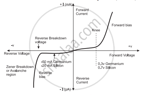
V-I Characteristics of a p-n Junction Diode
The graph of voltage across the diode versus current through the diode is known as the V-I characteristic of the p-n junction diode.
Forward characteristic
- For small forward voltages, the current is almost negligible.
- After the knee voltage, the current increases rapidly.
- The diode then behaves as a good conductor in the forward direction.
Reverse characteristic
- For reverse bias, only a small reverse saturation current flows initially.
- At very high reverse voltage, breakdown occurs and current rises sharply.
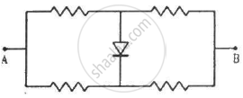
Example 1
Case 1: Diode is Forward Biased
- In forward bias, an ideal diode behaves like a closed switch (zero resistance), allowing current to flow.
- The circuit then has two 30 Ω resistors connected in parallel.
- The equivalent resistance is:
\[R_{AB}=\frac{30\times30}{30+30}=\frac{900}{60}=15\Omega\] - Therefore, the resistance between A and B is 15 Ω.
Case 2: Diode is Reverse Biased
- In reverse bias, an ideal diode behaves like an open switch (infinite resistance), so no current flows through that branch.
- The branch containing the diode is effectively disconnected.
- Current flows only through the remaining 30 Ω resistor.
- Therefore, the resistance between A and B is 30 Ω.
Final Answer
- Forward biased: RAB = 15 Ω
- Reverse biased: RAB = 30 Ω
Example 2
Can a p-type and an n-type semiconductor be physically joined to form a p-n junction?
Answer: No.
- A p-n junction cannot be formed by simply placing a p-type slab against an n-type slab.
- Even if both surfaces appear smooth, they have microscopic roughness that is much larger than the spacing between atoms (about 2–3 Å).
- Because of this roughness, the atoms of the two slabs do not make continuous contact, preventing the formation of a proper crystal lattice.
- As a result, the interface acts as a discontinuity (barrier) to charge carriers, so a true p-n junction is not formed.
Conclusion:
A p-n junction is created by doping different regions of the same semiconductor crystal, not by physically joining separate p-type and n-type semiconductor pieces.
Maharashtra State Board: Class 11
Real-Life Application
- Rectifiers: Diodes are used in power supplies and chargers to convert AC into DC.
- Electronic switching: Diodes control the direction of current in circuits.
- Signal detection: Diodes are used in communication and detection circuits.
- Semiconductor devices: The p-n junction principle is used in LEDs, photodiodes, and many other electronic components.
Maharashtra State Board: Class 11
key points: Diode or p-n Junction
- A p-n junction is formed by joining p-type and n-type semiconductor regions in a single crystal.
- Diffusion of carriers creates a depletion region and barrier potential.
- A p-n junction diode conducts mainly in one direction.
- In forward bias, the barrier potential decreases, and the current becomes large.
- In reverse bias, the barrier potential increases and only a small minority-carrier current flows.
- In zero bias, the diffusion and drift currents balance, so the net current is zero.
- The knee voltage is about 0.3 V for germanium and 0.7 V for silicon.
- Static resistance is given by R = V/I, and dynamic resistance is given by rd = ΔV/ΔI.