Advertisements
Advertisements
प्रश्न
Write the two processes that take place in the formation of a p-n junction.
Name two important processes involved in the formation of a p-n junction diode.
Advertisements
उत्तर
The processes of "diffusion" and "drift" are critical in a p-n junction. When the p and n-sides come into contact, the majority of carriers "diffuse" from a high concentration to a low concentration. Electrons move and combine with holes from the n-side to the p-side. Holes migrate from the p-side to the n-side in the same way that electrons and holes do at the junction. A "depletion region" is formed when the near junction area runs out of carriers and becomes charged. Current "diffusion" is caused by current "diffusion."
In the depletion area, the charge produces an electric field. The electric field creates a flow of minority carriers in the 'depletion' region. The produced current is known as "drift current," and it is referred to as drift. The directions of "diffusion and drift current" are reversed.
APPEARS IN
संबंधित प्रश्न
Explain briefly with the help of necessary diagrams, the reverse biasing of a p-n junction diode. Also draw characteristic curves.
The diffusion current in a p-n junction is
Two identical p-n junction may be connected in series with a battery in three ways. The potential difference across the two p-n junctions are equal in

The potential barrier existing across an unbiased p-n junction is 0.2 volt. What minimum kinetic energy a hole should have to diffuse from the p-side to the n-side if (a) the junction is unbiased, (b) the junction is forward-biased at 0.1 volt and (c) the junction is reverse-biased at 0.1 volt?
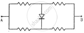
Each of the resistance shown in figure has a value of 20 Ω. Find the equivalent resistance between A and B. Does it depend on whether the point A or B is at higher potential?
Find the current through the resistance R in figure if (a) R = 12Ω (b) R = 48Ω.
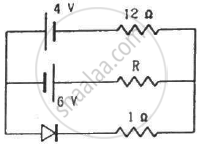
(Assume that the resistance of each diode is zero in forward bias and is infinity in reverse bias.)
Answer in detail.
Discuss the effect of external voltage on the width of depletion region of a p-n junction.
The formation of the depletion region in a p-n junction diode is due to ______.
How is a true p-n junction created instead of physically joining separate semiconductor pieces?
What role do diodes perform in electronic switching?
