Advertisements
Advertisements
Question
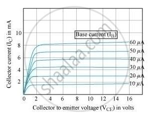
Draw a circuit diagram to study the input and output characteristics of an n-p-n transistor in its common emitter configuration. Draw the typical input and output characteristics.
Advertisements
Solution


APPEARS IN
RELATED QUESTIONS
In an unbiased p-n junction, holes diffuse from the p-region to n-region because ______.
Write the two processes that take place in the formation of a p-n junction.
When a p-type impurity is doped in a semiconductor, a large number of holes are created, This does not make the semiconductor charged. But when holes diffuse from the p-side to the n-side in a p-n junction, the n-side gets positively charged. Explain.
The diffusion current in a p-n junction is
In a p-n junction with open ends,
(a) there is no systematic motion of charge carries
(b) holes and conduction electrons systematically go from the p-side to n-side and from the n-side to p-side respectively
(c) there is no net charge transfer between the two sides
(d) there is a constant electric field near the junction.
What are the readings of the ammeters A1 and A2 shown in figure. Neglect the resistance of the meters.

(Assume that the resistance of each diode is zero in forward bias and is infinity in reverse bias.)
When the base current in a transistor is changed from 30µA to 80µA, the collector current is changed from 1.0 mA to 3.5 mA. Find the current gain β.
A diode, a resistor and a 50 Hz AC source are connected in series. The number of current pulses per second through the resistor is __________ .
Choose the correct option.
Current through a reverse-biased p-n junction increases abruptly at:
Zener breakdown occurs in a p-n junction having p and n both:
