Advertisements
Advertisements
प्रश्न
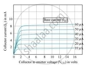
Draw a circuit diagram to study the input and output characteristics of an n-p-n transistor in its common emitter configuration. Draw the typical input and output characteristics.
Advertisements
उत्तर


APPEARS IN
संबंधित प्रश्न
In an unbiased p-n junction, holes diffuse from the p-region to n-region because ______.
Mention the important considerations required while fabricating a p-n junction diode to be used as a Light Emitting Diode (LED). What should be the order of band gap of an LED if it is required to emit light in the visible range?
How is a zener diode fabricated so as to make it a special purpose diode? Draw I-V characteristics of zener diode and explain the significance of breakdown voltage.
Explain briefly, with the help of a circuit diagram, how a p-n junction diode works as a half wave rectifier.
If the two ends of a p-n junction are joined by a wire,
The diffusion current in a p-n junction is
In a p.n junction, the depletion region is 400 nm wide and an electric field of 5 × 10⁵ V m−1 exists in it. (a) Find the height of the potential barrier. (b) What should be the minimum kinetic energy of a conduction electron which can diffuse from the n-side to the p-side?
The current−voltage characteristic of an ideal p-n junction diode is given by \[i = i_0 ( e^{eV/KT} - 1)\] where, the drift current i0 equals 10 µA. Take the temperature T to be 300 K. (a) Find the voltage V0 for which \[e^{eV/kT} = 100 .\]One can neglect the term 1 for voltages greater than this value. (b) Find an expression for the dynamic resistance of the diode as a function of V for V > V0. (c) Find the voltage for which the dynamic resistance is 0.2 Ω.
(Use Planck constant h = 4.14 × 10⁻¹⁵ eV-s, Boltzmann constant k = 8·62 × 10-5 eV/K.)
Consider a p-n junction diode having the characteristic \[i - i_0 ( e^{eV/kT} - 1) \text{ where } i_0 = 20\mu A\] . The diode is operated at T = 300 K . (a) Find the current through the diode when a voltage of 300 mV is applied across it in forward bias. (b) At what voltage does the current double?
Calculate the current through the circuit and the potential difference across the diode shown in figure. The drift current for the diode is 20 µA.

p-n junction diode is formed
