Advertisements
Advertisements
प्रश्न
Explain briefly with the help of necessary diagrams, the reverse biasing of a p-n junction diode. Also draw characteristic curves.
Advertisements
उत्तर
p-n junction diode under reverse bias
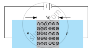
Positive terminal of battery is connected to n-side and negative terminal to p-side.
Reverse bias supports the potential barrier. Therefore, the barrier height increases and the width of depletion region also increases.
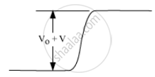
Effective barrier height under reverse bias is (V0 + V).
No conduction across the junction due to majority carriers; few minority carriers cross the junction after being accelerated by high reverse bias voltage
This constitutes a current that flows in opposite direction − celled reverse current.
APPEARS IN
संबंधित प्रश्न
Write the two processes that take place in the formation of a p-n junction.
A zener diode is fabricated by heavily doping both p- and n- sides of the junction. Explain, why?
Explain, with the help of a circuit diagram, the working of n-p-n transistor as a common emitter amplifier.
How is a zener diode fabricated so as to make it a special purpose diode? Draw I-V characteristics of zener diode and explain the significance of breakdown voltage.
Explain briefly, with the help of a circuit diagram, how a p-n junction diode works as a half wave rectifier.
A hole diffuses from the p-side to the n-side in a p-n junction. This means that
In a p-n junction,
(a) new holes and conduction electrons are produced continuously throughout the material
(b) new holes and conduction electrons are produced continuously throughout the material except in the depletion region
(c) holes and conduction electrons recombine continuously throughout the material
(d) holes and conduction electrons recombine continuously throughout the material except in the depletion region.
In a p-n junction, a potential barrier of 250 meV exists across the junction. A hole with a kinetic energy of 300 meV approaches the junction. Find the kinetic energy of the hole when it crosses the junction if the hole approached the junction (a) from the p-side and (b) from the n-side.
Find the currents through the resistance in the circuits shown in figure.

(Assume that the resistance of each diode is zero in forward bias and is infinity in reverse bias.)
Answer in detail.
Discuss the effect of external voltage on the width of depletion region of a p-n junction.
p-n junction diode is formed
