Advertisements
Advertisements
Question
Explain briefly with the help of necessary diagrams, the reverse biasing of a p-n junction diode. Also draw characteristic curves.
Advertisements
Solution
p-n junction diode under reverse bias
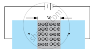
Positive terminal of battery is connected to n-side and negative terminal to p-side.
Reverse bias supports the potential barrier. Therefore, the barrier height increases and the width of depletion region also increases.
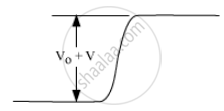
Effective barrier height under reverse bias is (V0 + V).
No conduction across the junction due to majority carriers; few minority carriers cross the junction after being accelerated by high reverse bias voltage
This constitutes a current that flows in opposite direction − celled reverse current.
APPEARS IN
RELATED QUESTIONS
In a p-n junction diode, the current I can be expressed as
I = `"I"_0 exp ("eV"/(2"k"_"BT") - 1)`
where I0 is called the reverse saturation current, V is the voltage across the diode and is positive for forward bias and negative for reverse bias, and I is the current through the diode, kBis the Boltzmann constant (8.6×10⁻⁵ eV/K) and T is the absolute temperature. If for a given diode I0 = 5 × 10⁻¹² A and T = 300 K, then
(a) What will be the forward current at a forward voltage of 0.6 V?
(b) What will be the increase in the current if the voltage across the diode is increased to 0.7 V?
(c) What is the dynamic resistance?
(d) What will be the current if reverse bias voltage changes from 1 V to 2 V?
Explain, with the help of a circuit diagram, the working of a photo-diode. Write briefly how it is used to detect the optical signals.
When a p-type impurity is doped in a semiconductor, a large number of holes are created, This does not make the semiconductor charged. But when holes diffuse from the p-side to the n-side in a p-n junction, the n-side gets positively charged. Explain.
The drift current in a reverse-biased p-n junction is increased in magnitude if the temperature of the junction is increased. Explain this on the basis of creation of hole-electron pairs.
A hole diffuses from the p-side to the n-side in a p-n junction. This means that
Consider a p-n junction diode having the characteristic \[i - i_0 ( e^{eV/kT} - 1) \text{ where } i_0 = 20\mu A\] . The diode is operated at T = 300 K . (a) Find the current through the diode when a voltage of 300 mV is applied across it in forward bias. (b) At what voltage does the current double?
Calculate the current through the circuit and the potential difference across the diode shown in figure. The drift current for the diode is 20 µA.

Find the current through the resistance R in figure if (a) R = 12Ω (b) R = 48Ω.

(Assume that the resistance of each diode is zero in forward bias and is infinity in reverse bias.)
Draw the current-voltage characteristics for the device show in figure between the terminals A and B.

(Assume that the resistance of each diode is zero in forward bias and is infinity in reverse bias.)
The depletion layer in the p-n junction diode is caused by ______.
