Advertisements
Advertisements
Question
In a p-n junction diode, the current I can be expressed as
I = `"I"_0 exp ("eV"/(2"k"_"BT") - 1)`
where I0 is called the reverse saturation current, V is the voltage across the diode and is positive for forward bias and negative for reverse bias, and I is the current through the diode, kBis the Boltzmann constant (8.6×10⁻⁵ eV/K) and T is the absolute temperature. If for a given diode I0 = 5 × 10⁻¹² A and T = 300 K, then
(a) What will be the forward current at a forward voltage of 0.6 V?
(b) What will be the increase in the current if the voltage across the diode is increased to 0.7 V?
(c) What is the dynamic resistance?
(d) What will be the current if reverse bias voltage changes from 1 V to 2 V?
Advertisements
Solution
a) In a p-n junction diode, the expression for current is given as:
I = `"I"_0 exp("eV"/(2"k"_"B" "T") - 1)`
Where,
I0 = Reverse saturation current = 5 × 10⁻¹² A
T = Absolute temperature = 300 K
kB = Boltzmann constant = 8.6 × 10⁻⁵ eV/K = 1.376 × 10⁻²³ J K−1
V = Voltage across the diode
(a) Forward voltage, V = 0.6 V
= `5 xx 10^(-12)[exp ((1.6xx 10^(-19) xx 0.6)/(1.376 xx 10^(-23) xx 300))-1]`
∴ Current, I
`= 5 xx 10^(-12) xx exp [22.36] = 0.0256 A`
Therefore, the forward current is about 0.0256 A.
(b) For forward voltage, V’ = 0.7 V, we can write:
I' =`5 xx 10^(-12) [exp ((1.6 xx 10^(-19) xx 0.7)/(1.376 xx 10^(-23) xx 300)) - 1]`
`= 5 xx 10^(-12) xx exp [26.25] = 1.257` A
Hence, the increase in current, ΔI = I' − I
= 1.257 − 0.0256 = 1.23 A
(c) Dynamic resistance = `"Change in voltage"/"Change in Current"`
`= (0.7 - 0.6)/1.23 = 0.1/1.23 = 0.081 "Ω"`
(d) If the reverse bias voltage changes from 1 V to 2 V, then the current (I) will almost remain equal to I0 in both cases. Therefore, the dynamic resistance in the reverse bias will be infinite.
RELATED QUESTIONS
Write the two processes that take place in the formation of a p-n junction.
Explain briefly with the help of necessary diagrams, the reverse biasing of a p-n junction diode. Also draw characteristic curves.
Explain, with the help of a circuit diagram, the working of a photo-diode. Write briefly how it is used to detect the optical signals.
Draw a circuit diagram to study the input and output characteristics of an n-p-n transistor in its common emitter configuration. Draw the typical input and output characteristics.
The drift current in a reverse-biased p-n junction is increased in magnitude if the temperature of the junction is increased. Explain this on the basis of creation of hole-electron pairs.
The drift current in a p-n junction is
Two identical p-n junction may be connected in series with a battery in three ways. The potential difference across the two p-n junctions are equal in

A semiconducting device is connected in a series circuit with a battery and a resistance. A current is found to pass through the circuit. If the polarity of the battery is reversed, the current drops to almost zero. the device may be
(a) an intrinsic semiconductor
(b) a p-type semiconductor
(c) an n-type semiconductor
(d) a p-n junction
Consider a p-n junction diode having the characteristic \[i - i_0 ( e^{eV/kT} - 1) \text{ where } i_0 = 20\mu A\] . The diode is operated at T = 300 K . (a) Find the current through the diode when a voltage of 300 mV is applied across it in forward bias. (b) At what voltage does the current double?
What are the readings of the ammeters A1 and A2 shown in figure. Neglect the resistance of the meters.
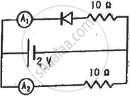
(Assume that the resistance of each diode is zero in forward bias and is infinity in reverse bias.)
Find the current through the resistance R in figure if (a) R = 12Ω (b) R = 48Ω.
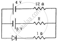
(Assume that the resistance of each diode is zero in forward bias and is infinity in reverse bias.)
Draw the current-voltage characteristics for the device show in figure between the terminals A and B.
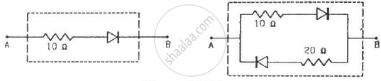
(Assume that the resistance of each diode is zero in forward bias and is infinity in reverse bias.)
Choose the correct option.
Current through a reverse-biased p-n junction increases abruptly at:
The depletion layer in the p-n junction diode is caused by ______.
What is the depletion region?
What is a p-n junction diode?
Which process moves charge carriers from a higher concentration to a lower concentration?
What is the net current in zero bias when diffusion and drift currents balance?
What is the approximate knee voltage for germanium?
