Advertisements
Advertisements
Question
Mention the important considerations required while fabricating a p-n junction diode to be used as a Light Emitting Diode (LED). What should be the order of band gap of an LED if it is required to emit light in the visible range?
Advertisements
Solution
1. The reverse breakdown voltages of LEDs are very low, typically around 5V. So care should be taken while fabricating a pn-junction diode so that the high reverse voltages do not appear across them.
2. There is very little resistance to limit the current in LED. Therefore, a resistor must be used in series with the LED to avoid any damage to it.
The semiconductor used for fabrication of visible LEDs must at least have a band gap of 1.8 eV (spectral range of visible light is from about 0.4 μm to 0.7 μm, i.e., from about 3 eV to 1.8 eV).
APPEARS IN
RELATED QUESTIONS
When a p-type impurity is doped in a semiconductor, a large number of holes are created, This does not make the semiconductor charged. But when holes diffuse from the p-side to the n-side in a p-n junction, the n-side gets positively charged. Explain.
A hole diffuses from the p-side to the n-side in a p-n junction. This means that
The current−voltage characteristic of an ideal p-n junction diode is given by \[i = i_0 ( e^{eV/KT} - 1)\] where, the drift current i0 equals 10 µA. Take the temperature T to be 300 K. (a) Find the voltage V0 for which \[e^{eV/kT} = 100 .\]One can neglect the term 1 for voltages greater than this value. (b) Find an expression for the dynamic resistance of the diode as a function of V for V > V0. (c) Find the voltage for which the dynamic resistance is 0.2 Ω.
(Use Planck constant h = 4.14 × 10⁻¹⁵ eV-s, Boltzmann constant k = 8·62 × 10-5 eV/K.)
Draw the current-voltage characteristics for the device show in figure between the terminals A and B.
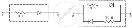
(Assume that the resistance of each diode is zero in forward bias and is infinity in reverse bias.)
A load resistor of 2kΩ is connected in the collector branch of an amplifier circuit using a transistor in common-emitter mode. The current gain β = 50. The input resistance of the transistor is 0.50 kΩ. If the input current is changed by 50µA. (a) by what amount does the output voltage change, (b) by what amount does the input voltage change and (c) what is the power gain?
p-n junction diode is formed
The formation of the depletion region in a p-n junction diode is due to ______.
How is a true p-n junction created instead of physically joining separate semiconductor pieces?
What is the use of diodes in power supplies and chargers?
Which formula gives the static resistance of a diode?
