Advertisements
Advertisements
Question
The drift current in a reverse-biased p-n junction is increased in magnitude if the temperature of the junction is increased. Explain this on the basis of creation of hole-electron pairs.
Advertisements
Solution
When the temperature of a reverse-biassed p‒n junction is increased, the breaking of bonds takes place because of the increase in the thermal energy of the charge carriers. Drift current is due to the flow of the minority carriers across the junction. So, when a p‒n junction is reverse biassed, the applied voltage supports the flow of minority charge carriers across the junction. Thus, the drift current increases with increase in temperature in a reverse-biassed p‒n junction.
APPEARS IN
RELATED QUESTIONS
A zener diode is fabricated by heavily doping both p- and n- sides of the junction. Explain, why?
A student wants to use two p-n junction diodes to convert alternating current into direct current. Draw the labelled circuit diagram she would use and explain how it works.
Explain, with the help of a circuit diagram, the working of a photo-diode. Write briefly how it is used to detect the optical signals.
Draw a circuit diagram to study the input and output characteristics of an n-p-n transistor in its common emitter configuration. Draw the typical input and output characteristics.
When a p-type impurity is doped in a semiconductor, a large number of holes are created, This does not make the semiconductor charged. But when holes diffuse from the p-side to the n-side in a p-n junction, the n-side gets positively charged. Explain.
Diffusion current in a p-n junction is greater than the drift current in magnitude
A hole diffuses from the p-side to the n-side in a p-n junction. This means that
In a p-n junction,
(a) new holes and conduction electrons are produced continuously throughout the material
(b) new holes and conduction electrons are produced continuously throughout the material except in the depletion region
(c) holes and conduction electrons recombine continuously throughout the material
(d) holes and conduction electrons recombine continuously throughout the material except in the depletion region.
In a p-n junction, a potential barrier of 250 meV exists across the junction. A hole with a kinetic energy of 300 meV approaches the junction. Find the kinetic energy of the hole when it crosses the junction if the hole approached the junction (a) from the p-side and (b) from the n-side.
Each of the resistance shown in figure has a value of 20 Ω. Find the equivalent resistance between A and B. Does it depend on whether the point A or B is at higher potential?
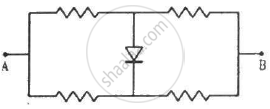
What are the readings of the ammeters A1 and A2 shown in figure. Neglect the resistance of the meters.
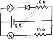
(Assume that the resistance of each diode is zero in forward bias and is infinity in reverse bias.)
When the base current in a transistor is changed from 30µA to 80µA, the collector current is changed from 1.0 mA to 3.5 mA. Find the current gain β.
A diode, a resistor and a 50 Hz AC source are connected in series. The number of current pulses per second through the resistor is __________ .
What is the depletion region?
Which charge carriers remain near the junction after the region loses mobile charge carriers?
Why does microscopic roughness prevent a proper crystal lattice from forming between separate p-type and n-type slabs?
What is the approximate knee voltage for germanium?
What is the approximate knee voltage for silicon?
Which formula gives the static resistance of a diode?
Which formula gives the dynamic resistance of a diode?
