Advertisements
Advertisements
प्रश्न
A zener diode is fabricated by heavily doping both p- and n- sides of the junction. Explain, why?
Advertisements
उत्तर
It is a heavily doped p-n junction. As a result, the depletion region formed is very thin and the electric field of the junction is extremely high even for a small reverse bias voltage.
The I-V characteristics of a Zener diode are shown in the figure below:

APPEARS IN
संबंधित प्रश्न
Explain, with the help of a circuit diagram, the working of a photo-diode. Write briefly how it is used to detect the optical signals.
How is a zener diode fabricated so as to make it a special purpose diode? Draw I-V characteristics of zener diode and explain the significance of breakdown voltage.
Explain briefly, with the help of a circuit diagram, how a p-n junction diode works as a half wave rectifier.
Diffusion current in a p-n junction is greater than the drift current in magnitude
In a p-n junction,
(a) new holes and conduction electrons are produced continuously throughout the material
(b) new holes and conduction electrons are produced continuously throughout the material except in the depletion region
(c) holes and conduction electrons recombine continuously throughout the material
(d) holes and conduction electrons recombine continuously throughout the material except in the depletion region.
Draw the current-voltage characteristics for the device show in figure between the terminals A and B.
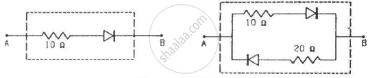
(Assume that the resistance of each diode is zero in forward bias and is infinity in reverse bias.)
When the base current in a transistor is changed from 30µA to 80µA, the collector current is changed from 1.0 mA to 3.5 mA. Find the current gain β.
A diode, a resistor and a 50 Hz AC source are connected in series. The number of current pulses per second through the resistor is __________ .
What is drift?
What is dynamic resistance?
In which circuits are diodes used for signal detection?
