Advertisements
Advertisements
Question
Find the equivalent resistance of the network shown in figure between the points A and B.
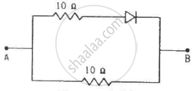
(Assume that the resistance of each diode is zero in forward bias and is infinity in reverse bias.)
Advertisements
Solution
Let the potentials at A and B be VA and VB, respectively.
(i) When VA > VB, that is, a battery is connected between points A and B, with its positive terminal connected to point A and its negative terminal connected to point B:
As the potential on the p-side of the diode is greater than the potential on the n-side of the diode, the diode is forward biased; thus, it can be replaced by a short circuit.
As the two resistances are connected in parallel, the effective resistance becomes
Equivalent resistance \[= \frac{10}{2} = 5 \Omega\]
(ii) When VA < VB:
The diode is reverse biased, so it is replaced by an open circuit. Thus, no current flows through this branch.
∴ Equivalent resistance = 10 Ω
APPEARS IN
RELATED QUESTIONS
Explain briefly with the help of necessary diagrams, the forward biasing of a p-n junction diode. Also draw characteristic curves.
Explain briefly with the help of necessary diagrams, the reverse biasing of a p-n junction diode. Also draw characteristic curves.
Mention the important considerations required while fabricating a p-n junction diode to be used as a Light Emitting Diode (LED). What should be the order of band gap of an LED if it is required to emit light in the visible range?
Draw a circuit diagram to study the input and output characteristics of an n-p-n transistor in its common emitter configuration. Draw the typical input and output characteristics.
The drift current in a p-n junction is
In a p-n junction,
(a) new holes and conduction electrons are produced continuously throughout the material
(b) new holes and conduction electrons are produced continuously throughout the material except in the depletion region
(c) holes and conduction electrons recombine continuously throughout the material
(d) holes and conduction electrons recombine continuously throughout the material except in the depletion region.
Find the current through the battery in each of the circuits shown in figure.
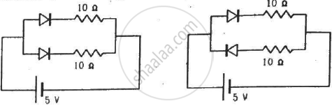
(Assume that the resistance of each diode is zero in forward bias and is infinity in reverse bias.)
Draw the current-voltage characteristics for the device show in figure between the terminals A and B.
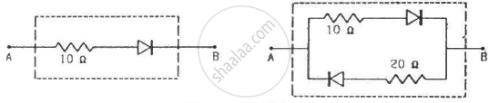
(Assume that the resistance of each diode is zero in forward bias and is infinity in reverse bias.)
When the base current in a transistor is changed from 30µA to 80µA, the collector current is changed from 1.0 mA to 3.5 mA. Find the current gain β.
An AC source is connected to a diode and a resistor in series. Is the current thorough the resistor AC or DC?
During the formation of a p-n junction ______.
Diode and resistance are connected as shown in figure. Out of the following statements which one is TRUE?
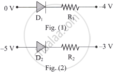
What is barrier potential?
What is drift?
How is a true p-n junction created instead of physically joining separate semiconductor pieces?
What is the use of diodes in power supplies and chargers?
What role do diodes perform in electronic switching?
What is the net current in zero bias when diffusion and drift currents balance?
What is the approximate knee voltage for germanium?
