Definitions [29]
A pure semiconductor in which no impurity is added intentionally.
The vacancy left in the valence band when an electron leaves it behaves like a positive charge carrier in semiconductor theory.
The concentration of charge carriers in an intrinsic semiconductor, where the number of electrons equals the number of holes.
The semiconductor to which the dopant is added is called the host.
Intrinsic semiconductors have very low conductivity at room temperature. Therefore, they are not useful for constructing electronic devices. Their electrical conductivity can be increased by adding a suitable impurity. This process is called doping.
A doped semiconductor is called an extrinsic semiconductor or impurity semiconductor.
The impurity added is called a dopant.
Since every pentavalent dopant atom donates one electron for conduction, it is called a donor impurity.
A p-type semiconductor is a semiconductor obtained by doping pure silicon or germanium with a trivalent impurity so that holes become the majority charge carriers.
The process in which charge carriers move from a higher concentration to a lower concentration is called diffusion.
The motion of charge carriers under the influence of an electric field is called drift.
The minimum forward voltage after which the current rises sharply is called the knee voltage.
The small current flowing in reverse bias due to minority carriers is called the reverse saturation current.
The reverse voltage at which the current suddenly increases rapidly is called the breakdown voltage.
The ratio of voltage to current at any operating point of a diode is called static resistance.
The ratio of a small change in voltage to the corresponding small change in current is called dynamic resistance.
The boundary formed when p-type and n-type semiconductor regions are joined in a single crystal is called a p-n junction.
The potential difference developed across the depletion layer due to immobile ions is called the barrier potential.
The region around the junction that is free from mobile charge carriers is called the depletion region.
The two-terminal semiconductor device that allows current mainly in one direction is called a p-n junction diode.
With reference to a semiconductor diode, define the depletion region.
A semiconductor diode's depletion zone is the area surrounding the p-n junction where there are no mobile charge carriers, this area generates an electric field that allows the diode to conduct in one direction while blocking in another.
With reference to a semiconductor diode, define the potential barrier.
The barrier that the repelling forces use to stop the mobile charge carriers (at the PN junction) is known as the potential barrier.
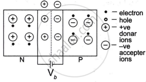
This results from the concentration of immobile charges close to the junction after electrons and holes diffuse across the function.
In semiconductor physics, what is meant by:
(i) rectifier
(ii) an amplifier
(iii) an oscillator
(i) Rectifier: It is a device which converts alternating current into direct current.
(ii) Amplifier: An amplifier is a device which increases the energy of a weak signal by supplying energy from an external source. An amplifier increases the amplitude of a input signal.
(iii) Oscillator: An oscillator is a device which produces electrical oscillations of adjustable frequency and constant amplitude. An oscillator is basically an amplifier. A part of the output energy is fed back into the L-C circuit to produce sustained oscillations.
A semiconductor diode is a two-terminal p-n junction device that allows current to pass easily in one direction and offers high resistance in the opposite direction.
A rectifier is an electronic circuit that converts alternating current (AC) into direct current (DC) by using one or more p-n junction diodes.
A half-wave rectifier allows only one half of the AC cycle to pass through the load, producing a pulsating DC output.
A full-wave rectifier uses both half cycles of the AC input to produce a more continuous pulsating DC output.
A filter is a circuit element or arrangement, often involving a capacitor or inductor, used to smooth the pulsating rectified output.
Pulsating DC is an output that flows in one direction but whose magnitude changes with time.
Formulae [3]
If hole concentration is high, then:
This is especially important for numerical problems in board examinations and entrance tests.
R = \[\frac {V}{I}\]
\[r_d=\frac{\Delta V}{\Delta I}\]
Theorems and Laws [1]
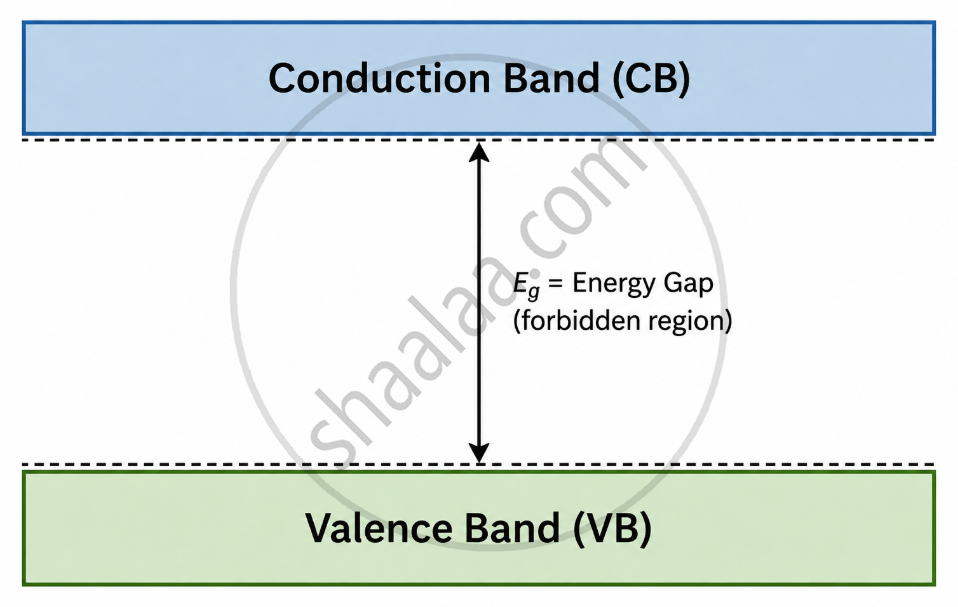
Formation of Energy Bands
In a single isolated atom, electrons occupy discrete, well-defined energy levels (like rungs of a ladder).
When atoms are packed together in a crystal lattice, electrons are shared among neighbouring atoms. This causes:
- Each discrete energy level splits into closely spaced levels
- These closely spaced levels collectively form an energy band
Analogy: Think of a single tuning fork producing one frequency. When thousands of tuning forks are placed close together, they create a continuous range (band) of frequencies, not a single note.
Key Energy Bands
| Band | Description |
|---|---|
| Valence Band (VB) | The highest-energy band that is completely or partially filled with electrons at 0 K. Electrons here are bound to atoms. |
| Forbidden Energy Gap (E_g) | Energy region with no allowed states. Electrons cannot exist here. Also called the Band Gap. |
| Conduction Band (CB) | Energy band above the valence band. Electrons here are free to move and conduct electricity. |
Key Points
- Electronic circuits are built using devices that allow controlled flow of electrons.
- Before 1948, vacuum tubes or valves were commonly used.
- Electrons in vacuum tubes come from a heated cathode and move in the vacuum.
- Vacuum tube devices are bulky, high-power, high-voltage, with limited lifetime and low reliability.
- Semiconductor devices work within the solid itself.
- Semiconductor devices do not require external heating or a large evacuated space.
- Semiconductor devices are small, low-power, low-voltage, long-life, and highly reliable.
- Intrinsic semiconductors have very low conductivity at room temperature.
- Doping increases conductivity.
- A doped semiconductor is called an extrinsic semiconductor.
- The impurity added is called a dopant.
- The semiconductor receiving the impurity is called the host.
- The dopant size should be nearly the same as that of the host atom.
- Pentavalent and trivalent impurities are used as dopants.
- Extrinsic semiconductors are of two types: n-type and p-type.
- An n-type semiconductor is formed by doping silicon or germanium with a pentavalent impurity.
- Pentavalent impurities act as donor impurities.
- The fifth valence electron is weakly bound and can become free easily.
- Electrons are majority carriers and holes are minority carriers.
- For an n-type semiconductor, ne >> nh.
- Donor energy levels lie close to the conduction band.
- Extrinsic semiconductors are better conductors than intrinsic semiconductors.
- A p-n junction is formed by joining p-type and n-type semiconductor regions in a single crystal.
- Diffusion of carriers creates a depletion region and barrier potential.
- A p-n junction diode conducts mainly in one direction.
- In forward bias, the barrier potential decreases, and the current becomes large.
- In reverse bias, the barrier potential increases and only a small minority-carrier current flows.
- In zero bias, the diffusion and drift currents balance, so the net current is zero.
- The knee voltage is about 0.3 V for germanium and 0.7 V for silicon.
- Static resistance is given by R = V/I, and dynamic resistance is given by rd = ΔV/ΔI.
Important Questions [46]
- Draw an energy band diagram for an n-type semiconductor at T > 0 K.
- Draw an energy band diagram for a p-type semiconductor at T > 0 K.
- Three Photodiodes D1, D2, and D3 Are Made of Semiconductors Having Band Gaps of 2.5 Ev, 2 Ev, and 3 Ev Respectively. Which of Them Will Not Be Able to Detect Light of Wavelength 600 Nm?
- Two crystals C1 and C2, made of pure silicon, are doped with arsenic and aluminium respectively. Why is doping of intrinsic semiconductors necessary?
- What is meant by doping of an intrinsic semiconductor?
- Name the two types of atoms used for doping of Ge/Si.
- Assertion (A): The resistance of an intrinsic semiconductor decreases with an increase in its temperature. Reason (R): The number of conduction electrons as well as hole increase in an intrinsic
- Answer the following giving reasons: Impurities are added to intrinsic semiconductors.
- Two crystals C1 and C2, made of pure silicon, are doped with arsenic and aluminium respectively. Identify the extrinsic semiconductors so formed.
- Name the extrinsic semiconductors formed when pure germanium is doped with a trivalent impurity. Draw the energy band diagram of extrinsic semiconductors so formed.
- Name the extrinsic semiconductors formed when pure germanium is doped with a Pentavalent impurity. Draw the energy band diagram of extrinsic semiconductors so formed.
- In an extrinsic semiconductor, the number density of holes is 4 × 10²⁰ m-3. If the number density of intrinsic carriers is 1.2 × 10¹⁵ m-3, the number density of electrons in it is ______.
- Pieces of copper and of silicon are initially at room temperature. Both are heated to temperature T. The conductivity of ______.
- Distinguish Between 'Intrinsic' and 'Extrinsic' Semiconductors
- Explain Briefly with the Help of Necessary Diagrams, the Forward Biasing of a P-n Junction Diode. Also Draw Characteristic Curves.
- During the formation of a p-n junction ______.
- The formation of the depletion region in a p-n junction diode is due to ______.
- Explain briefly with the help of necessary diagrams, the reverse biasing of a p-n junction diode. Also draw characteristic curves.
- Draw a Circuit Diagram to Study the Input and Output Characteristics of an N-p-n Transistor in Its Common Emitter Configuration. Draw the Typical Input and Output Characteristics.
- Explain, with the Help of a Circuit Diagram, the Working of N-p-n Transistor as a Common Emitter Amplifier.
- How is a Zener Diode Fabricated So as to Make It a Special Purpose Diode? Draw I-v Characteristics of Zener Diode and Explain the Significance of Breakdown Voltage.Explain Briefly, with the Help of a
- Mention the Important Considerations Required While Fabricating a P-n Junction Diode to Be Used as a Light Emitting Diode (Led).
- Explain, with the Help of a Circuit Diagram, the Working of a Photo-diode. Write Briefly How It is Used to Detect the Optical Signals.
- A Student Wants to Use Two P-n Junction Diodes to Convert Alternating Current into Direct Current. Draw the Labelled Circuit Diagram She Would Use and Explain How It Works.
- Write the two processes that take place in the formation of a p-n junction.
- A Zener Diode is Fabricated by Heavily Doping Both P- and N- Sides of the Junction. Explain, Why?
- Describe the following term briefly: Breakdown voltage in reverse biasing
- What Happens When a Forward Bias is Applied to a P-N Junction?
- What Causes the Setting up of High Electric Field Even for Small Reverse Bias Voltage Across the Diode?
- In the following diagram 'S' is a semiconductor. Would you increase or decrease the value of R to keep the reading of the ammeter A constant when S is heated? Give reason for your answer.
- Draw its I – V characteristics of photodiode
- In the Following Diagram, is the Junction Diode Forward Biased Or Reverse Biased ?
- Plot a Graph Showing Variation of Current Versus Voltage for the Material Gaas ?
- The Graph Shown in the Figure Represents a Plot of Current Versus Voltage for a Given Semiconductor. Identify the Region, If Any, Over Which the Semiconductor Has a Negative Resistance.
- Show on a Graph, the Variation of Resistivity with Temperature for a Typical Semiconductor.
- Why is a Zener Diode Considered as a Special Purpose Semiconductor Diode?
- Answer the Following Question. Why Photodiodes Are Required to Operate in Reverse Bias? Explain.
- Draw V-I characteristics of a p-n Junction diode.
- Differentiate between the threshold voltage and the breakdown voltage for a diode.
- Write the property of a junction diode which makes it suitable for rectification of ac voltages.
- Explain the formation of the barrier potential in a p-n junction.
- Answer the following giving reasons: A p-n junction diode is damaged by a strong current.
- A semiconductor device is connected in series with a battery, an ammeter and a resistor. A current flows in the circuit. If. the polarity of the battery is reversed, the current in the circuit
- Draw the circuit arrangement for studying V-I characteristics of a p-n junction diode in (i) forward biasing and (ii) reverse biasing. Draw the typical V-I characteristics of a silicon diode.
- Describe the following term briefly: Minority carrier injection in forward biasing.
- Explain with the Help of a Diagram the Formation of Depletion Region and Barrier Potential in a Pn Junction.
