Advertisements
Advertisements
Questions
Describe the following term briefly:
Minority carrier injection in forward biasing.
Explain the following term:
Minority carrier injection in forward bias
Advertisements
Solution
Due to the applied voltage, electrons from the n-side cross the depletion region and reach the p-side (where they are minority carriers). Similarly, holes from the p-side cross this junction and reach the n-side (where they are minority carriers). This process under forward bias is known as minority carrier injection.
APPEARS IN
RELATED QUESTIONS
(i) Explain with the help of a diagram the formation of depletion region and barrier potential in a pn junction.
When a forward bias is applied to a p-n junction, it ______.
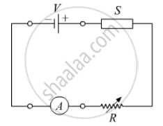
In the following diagram 'S' is a semiconductor. Would you increase or decrease the value of R to keep the reading of the ammeter A constant when S is heated? Give reason for your answer.
Draw its I – V characteristics of photodiode
Why is a zener diode considered as a special purpose semiconductor diode?
The expected energy of the electron at absolute zero is called:-
Avalanche breakdown is due to ______.
When an electric field is applied across a semiconductor ______.
- electrons move from lower energy level to higher energy level in the conduction band.
- electrons move from higher energy level to lower energy level in the conduction band.
- holes in the valence band move from higher energy level to lower energy level.
- holes in the valence band move from lower energy level to higher energy level.
Consider an npn transistor with its base-emitter junction forward biased and collector base junction reverse biased. Which of the following statements are true?
- Electrons crossover from emitter to collector.
- Holes move from base to collector.
- Electrons move from emitter to base.
- Electrons from emitter move out of base without going to the collector.
Draw a labelled characteristic curve (l-V graph) for a semiconductor diode during forward bias.
