Advertisements
Advertisements
Question
When an electric field is applied across a semiconductor ______.
- electrons move from lower energy level to higher energy level in the conduction band.
- electrons move from higher energy level to lower energy level in the conduction band.
- holes in the valence band move from higher energy level to lower energy level.
- holes in the valence band move from lower energy level to higher energy level.
Options
a and b
b and c
d and a
a and c
Advertisements
Solution
a and c
Explanation:
In the valence band electrons are not capable of gaining energy from the external electric fields. While in the conduction band the electrons can gain energy from the external electric field.
When an electric field is applied across a semiconductor, the electrons in the conduction band (which is partially filled with electrons) get accelerated and acquire energy. They move from lower energy levels to higher energy levels. While the holes in the valence band move from higher energy level to lower energy level, where they will be having more energy.
APPEARS IN
RELATED QUESTIONS
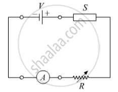
In the following diagram 'S' is a semiconductor. Would you increase or decrease the value of R to keep the reading of the ammeter A constant when S is heated? Give reason for your answer.
Draw its I – V characteristics of photodiode
Show on a graph, the variation of resistivity with temperature for a typical semiconductor.
A plate current of 10 mA is obtained when 60 volts are applied across a diode tube. Assuming the Langmuir-Child relation \[i_p \infty V_p^{3/2}\] to hold, find the dynamic resistance rp in this operating condition.
With reference to a semiconductor diode, what is meant by:
(i) Forward bias
(ii) Reverse bias
(iii) Depletion region
Basic materials used in the present solid state electronic devices like diode, transistor, ICs, etc are ______.
Of the diodes shown in the following diagrams, which one is reverse biased?
The nature of binding for a crystal with alternate and evenly spaced positive and negatively ions is
Use a transistor as an amplition
The expected energy of the electron at absolute zero is called:-
Avalanche breakdown is due to ______.
Figure shows the transfer characteristics of a base biased CE transistor. Which of the following statements are true?

At Vi = 0.4 V, transistor is in active state.
At Vi = 1 V, it can be used as an amplifier.
At Vi = 0.5 V, it can be used as a switch turned off.
At Vi = 2.5 V, it can be used as a switch turned on.
The breakdown in a reverse biased p–n junction diode is more likely to occur due to ______.
- large velocity of the minority charge carriers if the doping concentration is small.
- large velocity of the minority charge carriers if the doping concentration is large.
- strong electric field in a depletion region if the doping concentration is small.
- strong electric field in the depletion region if the doping concentration is large.
Can the potential barrier across a p-n junction be measured by simply connecting a voltmeter across the junction?
Consider a box with three terminals on top of it as shown in figure (a):
 (a) |
Three components namely, two germanium diodes and one resistor are connected across these three terminals in some arrangement. A student performs an experiment in which any two of these three terminals are connected in the circuit shown in figure (b).
 (b) |
The student obtains graphs of current-voltage characteristics for unknown combination of components between the two terminals connected in the circuit. The graphs are
(i) when A is positive and B is negative
 (c) |
(ii) when A is negative and B is positive
 (d) |
(iii) When B is negative and C is positive
|
(e) |

(iv) When B is positive and C is negative
 (f) |
(v) When A is positive and C is negative
 (g) |
(vi) When A is negative and C is positive
 (h) |
From these graphs of current-voltage characteristics shown in figure (c) to (h), determine the arrangement of components between A, B and C.
The graph of potential barrier versus width of depletion region for an unbiased diode is shown in graph A. In comparison to A, graphs B and C are obtained after biasing the diode in different ways. Identify the type of biasing in B and C and justify your answer
| ‘A’ | ‘B’ | ‘C’ |
 |
 |
 |
A semiconductor device is connected in series with a battery, an ammeter and a resistor. A current flows in the circuit. If. the polarity of the battery is reversed, the current in the circuit almost becomes zero. The device is a/an ______.
