Advertisements
Advertisements
Question
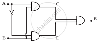
Truth table for the given circuit (Figure) is ______.
Options
A B E 0 0 1 0 1 0 1 0 1 1 1 0 A B E 0 0 1 0 1 0 1 0 0 1 1 1 A B E 0 0 1 0 1 1 1 0 0 1 1 1 A B E 0 0 0 0 1 1 1 0 1 1 1 0
MCQ
Fill in the Blanks
Advertisements
Solution
| A | B | E |
| 0 | 0 | 1 |
| 0 | 1 | 1 |
| 1 | 0 | 0 |
| 1 | 1 | 1 |
Explanation:
In this problem, the input C of the OR gate is an output of the AND gate. So, “C equals A AND B” or C = A · B and “D equals Not A AND B” or D = Ā · B and “E equals C AND D" or E = C + D = (A · B) + (A · B)
Now we can generate the truth table of this arrangement of gates can be given by
| A | B | Ā | C = A · B | d = Ā · B | E = (C + D) |
| 0 | 0 | 1 | 0 | 0 | 0 |
| 0 | 1 | 1 | 0 | 1 | 1 |
| 1 | 0 | 0 | 0 | 0 | 0 |
| 1 | 1 | 1 | 1 | 0 | 1 |
shaalaa.com
Is there an error in this question or solution?
