Advertisements
Advertisements
प्रश्न
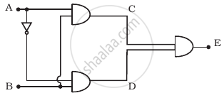
Truth table for the given circuit (Figure) is ______.

विकल्प
A B E 0 0 1 0 1 0 1 0 1 1 1 0 A B E 0 0 1 0 1 0 1 0 0 1 1 1 A B E 0 0 1 0 1 1 1 0 0 1 1 1 A B E 0 0 0 0 1 1 1 0 1 1 1 0
Advertisements
उत्तर
| A | B | E |
| 0 | 0 | 1 |
| 0 | 1 | 1 |
| 1 | 0 | 0 |
| 1 | 1 | 1 |
Explanation:
In this problem, the input C of the OR gate is an output of the AND gate. So, “C equals A AND B” or C = A · B and “D equals Not A AND B” or D = Ā · B and “E equals C AND D" or E = C + D = (A · B) + (A · B)
Now we can generate the truth table of this arrangement of gates can be given by
| A | B | Ā | C = A · B | d = Ā · B | E = (C + D) |
| 0 | 0 | 1 | 0 | 0 | 0 |
| 0 | 1 | 1 | 0 | 1 | 1 |
| 1 | 0 | 0 | 0 | 0 | 0 |
| 1 | 1 | 1 | 1 | 0 | 1 |
APPEARS IN
संबंधित प्रश्न
The output of NOR gate is high, when _______.
The logic gate which produces LOW output when one of the input is HIGH and produces
HIGH output only when all of its inputs are LOW is called _______.
(A) AND gate
(B) OR gate
(C) NOR gate
(D) NAND gate
You are given the two circuits as shown in following figure. Show that circuit
- acts as OR gate while the circuit
- acts as AND gate.
(a)

(b)

You are given two circuits as shown in following figure, which consist of NAND gates. Identify the logic operation carried out by the two circuits.
(a)

(b)

Draw logic symbol of an OR gate and write its truth table.
You are given a circuit below. Write its truth table. Hence, identify the logic operation carried out by this circuit. Draw the logic symbol of the gate it corresponds to.

What will be the values of input A and B for the Boolean expression `overline ((A +B) .(A*B)) =1?`
Let \[X = A \overline{ BC} + B\overline{ CA} + C\overline{AB } .\] Evaluate X for A = B = C = 0.
Why is the linear portion of the triode characteristic chosen to operate the triode as an amplifier?
(i) Write the truth tables of the logic gates marked P and Q in the given circuit.
(ii) Write the truth table for the circuit.

Why are NOR gates considered as universal gates?
With the help of a diagram, show how you can use several NAND gates to obtain an OR gate.
Useful Constants and Relations :
| 1. Speed of Light in Vacuum | (c) = 3.00 x 10⁸ m/s |
| 2. Charge of a proton | (e) = 1.60 x 10⁻¹⁹C |
| 3. Planck's Constant | (h) = 6.6 x 10⁻³⁴ Js |
| 4. Permeability of vacuum | (μ0) = 4π x 10-7 Hm-1 |
| 5. Electron Volt | (1eV ) = 1.6 x 10 |
| 6. Unified Atomic Mass Unit | (1u) = 931 MeV |
| (π) = 3.14 | |
| ( ln 2 ) = 0.693 |
The Boolean expression for NAND gate is
The truth table for the following logic circuit is:

In the logic circuit shown in the figure, if input A and B are 0 to 1 respectively, the output at Y would be 'x'. The value of x is ______.

Identify the logic operation carried out by the given circuit:

A logic gate circuit has two inputs A and B and output Y. The voltage waveforms of A, B and Y are shown below.

The logic gate circuit is ______.
