Advertisements
Advertisements
प्रश्न
In the circuit shown in figure, if the diode forward voltage drop is 0.3 V, the voltage difference between A and B is ______.

विकल्प
1.3 V
2.3 V
0
0.5 V
Advertisements
उत्तर
In the circuit shown in figure, if the diode forward voltage drop is 0.3 V, the voltage difference between A and B is 2.3 V.
Explanation:
Let us consider figure 2.3 V given above in the problem, suppose the potential difference between A and B is VAB.
Then, `V_(AB) - 0.3 = [(r_1 + r_2)10^3] xx (0.2 xx 10^-3)` .....[∵ VAB = ir]
= `[(5 + 5)10^3] xx (0.2 xx 10^-3)]`
= `10 xx 10^3 xx 0.2 xx 10^-3`
= 2
⇒ VAB = 2 + 0.3 = 2.3 V
APPEARS IN
संबंधित प्रश्न
When a forward bias is applied to a p-n junction, it ______.
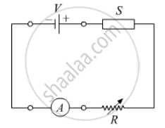
In the following diagram 'S' is a semiconductor. Would you increase or decrease the value of R to keep the reading of the ammeter A constant when S is heated? Give reason for your answer.
Draw its I – V characteristics of photodiode
In the following diagram, is the junction diode forward biased or reverse biased ?
The plate current in a diode is 20 mA when the plate voltage is 50 V or 60 V. What will be the current if the plate voltage is 70 V?
The gain factor of an amplifier in increased from 10 to 12 as the load resistance is changed from 4 kΩ to 8 kΩ. Calculate (a) the amplification factor and (b) the plate resistance.
The drift current in a p-n junction is from the ______.
A – pn junction has a depletion layer of thickness .of the order of
In a semiconductor diode, the barrier potential offers opposition to only
Figure shows the transfer characteristics of a base biased CE transistor. Which of the following statements are true?

At Vi = 0.4 V, transistor is in active state.
At Vi = 1 V, it can be used as an amplifier.
At Vi = 0.5 V, it can be used as a switch turned off.
At Vi = 2.5 V, it can be used as a switch turned on.
 (a) |
 (b) |
- Name the type of a diode whose characteristics are shown in figure (A) and figure (B).
- What does the point P in figure (A) represent?
- What does the points P and Q in figure (B) represent?
In the circuit shown in figure, when the input voltage of the base resistance is 10 V, Vbe is zero and Vce is also zero. Find the values of Ib, Ic and β.

Consider a box with three terminals on top of it as shown in figure (a):
 (a) |
Three components namely, two germanium diodes and one resistor are connected across these three terminals in some arrangement. A student performs an experiment in which any two of these three terminals are connected in the circuit shown in figure (b).
 (b) |
The student obtains graphs of current-voltage characteristics for unknown combination of components between the two terminals connected in the circuit. The graphs are
(i) when A is positive and B is negative
 (c) |
(ii) when A is negative and B is positive
 (d) |
(iii) When B is negative and C is positive
|
(e) |

(iv) When B is positive and C is negative
 (f) |
(v) When A is positive and C is negative
 (g) |
(vi) When A is negative and C is positive
 (h) |
From these graphs of current-voltage characteristics shown in figure (c) to (h), determine the arrangement of components between A, B and C.
Write the property of a junction diode which makes it suitable for rectification of ac voltages.
A semiconductor device is connected in series with a battery, an ammeter and a resistor. A current flows in the circuit. If. the polarity of the battery is reversed, the current in the circuit almost becomes zero. The device is a/an ______.
With reference to a semiconductor diode, define the depletion region.
An ideal PN junction diode offers ______.
A full wave rectifier circuit diodes (D1) and (D2) is shown in the figure. If input supply voltage Vin = 220 sin (100 πt) volt, then at t = 15 ms.

