Advertisements
Advertisements
प्रश्न
 (a) |
 (b) |
- Name the type of a diode whose characteristics are shown in figure (A) and figure (B).
- What does the point P in figure (A) represent?
- What does the points P and Q in figure (B) represent?
Advertisements
उत्तर
- Figure (a) represents the characteristics of the Zener diode and curve (b) is of the solar cell.
- In figure (a), point P represents Zener breakdown voltage.
- In figure (b), point Q represents zero voltage and negative current. This means the light falling on the solar cell with at least a minimum threshold frequency gives the current in opposite direction to that due to a battery connected to solar cell. But for point Q the battery is short-circuited. Hence it represents the short circuit current. And the point Pin fig. (b) represents some open circuit, the voltage on solar cell with zero current through solar cell.
It means, there is a battery connected to a solar cell which gives rise to the equal and opposite current to that in a solar cell by virtue of light falling on it.
APPEARS IN
संबंधित प्रश्न
When a forward bias is applied to a p-n junction, it ______.
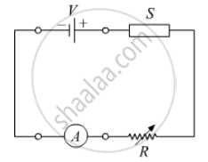
In the following diagram 'S' is a semiconductor. Would you increase or decrease the value of R to keep the reading of the ammeter A constant when S is heated? Give reason for your answer.
Draw its I – V characteristics of photodiode
What is the use of Zener diode?
The graph shown in the figure represents a plot of current versus voltage for a given semiconductor. Identify the region, if any, over which the semiconductor has a negative resistance.

In a photo diode, the conductive increases when the material is exposed to light. It is found that the conductivity changes only if the wavelength is less than 620 nm. What is the band gap?
(Use Planck constant h = 4.14 × 10⁻¹⁵ eV-s, Boltzmann constant k = 8·62 × 10-5 eV/K.)
The power delivered in the plate circular of a diode is 1.0 W when the plate voltage is 36 V. Find the power delivered if the plate voltage is increased to 49 V. Assume Langmuir-Child equation to hold.
Find the values of rp, µ and gm of a triode operating at plate voltage 200 V and grid voltage −6. The plate characteristics are shown in the figure.

We use alloys for making standard resistors because they have ____________.
With reference to Semiconductor Physics,
Name the diode that emits spontaneous radiation when forward biased.
The drift current in a p-n junction is from the ______.
Depletion layer in p - n junction diode consists of
The nature of binding for a crystal with alternate and evenly spaced positive and negatively ions is
Use a transistor as an amplition
On increasing the reverse biases voltage to a large value in a P – N junction diode-current
When an electric field is applied across a semiconductor ______.
- electrons move from lower energy level to higher energy level in the conduction band.
- electrons move from higher energy level to lower energy level in the conduction band.
- holes in the valence band move from higher energy level to lower energy level.
- holes in the valence band move from lower energy level to higher energy level.
Figure shows the transfer characteristics of a base biased CE transistor. Which of the following statements are true?

At Vi = 0.4 V, transistor is in active state.
At Vi = 1 V, it can be used as an amplifier.
At Vi = 0.5 V, it can be used as a switch turned off.
At Vi = 2.5 V, it can be used as a switch turned on.
Draw V-I characteristics of a p-n Junction diode.
Answer the following giving reasons:
A p-n junction diode is damaged by a strong current.
With reference to a semiconductor diode, define the potential barrier.
