Advertisements
Advertisements
प्रश्न
The power delivered in the plate circular of a diode is 1.0 W when the plate voltage is 36 V. Find the power delivered if the plate voltage is increased to 49 V. Assume Langmuir-Child equation to hold.
Advertisements
उत्तर
Given:-
When plate voltage, Vp, is 36 V, power delivered in the plate circular of a diode, P, is 1.0 W.
Let the plate current be Ip.
Let the power delivered be P' and plate current be Ip' when plate voltage, Vp, is increased to 49 V
\[ P = I_p V_p \]
\[ \Rightarrow I_p = \frac{P}{V_P} = \frac{1}{36}\]
According to Langmuir-Child equation,
\[I_p \propto ( V_p )^{3/2} , \]
\[ I_p ' \propto ( V_p ' )^{3/2} , \]
\[ \Rightarrow \frac{I_p}{I '_p} = \frac{( V_p )^{3/2}}{( V_p ' )^{3/2}}\]
\[ \Rightarrow \frac{1/36}{I_p '} = \left( \frac{36}{49} \right)^{3/2} \]
\[ \Rightarrow I_p = 0 . 04411\]
Thus, power delivered when the plate voltage is increased to 49 V,
\[P' = V_p ' \times I_p '\]
\[P' = 49 \times 0 . 04411 W\]
\[P' = 2 . 1613 W = 2 . 2 W\]
APPEARS IN
संबंधित प्रश्न
Draw a labelled diagram of a full wave rectifier. Show how output voltage varies with time if the input voltage is a sinusoidal voltage.
The graph shown in the figure represents a plot of current versus voltage for a given semiconductor. Identify the region, if any, over which the semiconductor has a negative resistance.

Why is a zener diode considered as a special purpose semiconductor diode?
The dynamic plate resistance of a triode value is 10 kΩ. Find the change in the plate current if the plate voltage is changed from 200 V to 220 V.
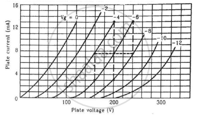
Find the values of rp, µ and gm of a triode operating at plate voltage 200 V and grid voltage −6. The plate characteristics are shown in the figure.
The gain factor of an amplifier in increased from 10 to 12 as the load resistance is changed from 4 kΩ to 8 kΩ. Calculate (a) the amplification factor and (b) the plate resistance.
With reference to a semiconductor diode, what is meant by:
(i) Forward bias
(ii) Reverse bias
(iii) Depletion region
The drift current in a p-n junction is from the ______.
Avalanche breakdown is due to ______.
In Figure, Vo is the potential barrier across a p-n junction, when no battery is connected across the junction ______.

Figure shows the transfer characteristics of a base biased CE transistor. Which of the following statements are true?

At Vi = 0.4 V, transistor is in active state.
At Vi = 1 V, it can be used as an amplifier.
At Vi = 0.5 V, it can be used as a switch turned off.
At Vi = 2.5 V, it can be used as a switch turned on.
 (a) |
 (b) |
- Name the type of a diode whose characteristics are shown in figure (A) and figure (B).
- What does the point P in figure (A) represent?
- What does the points P and Q in figure (B) represent?
Differentiate between the threshold voltage and the breakdown voltage for a diode.
Write the property of a junction diode which makes it suitable for rectification of ac voltages.
What current flows in the reverse-bias V-I characteristic before breakdown?
What happens to reverse current at the breakdown voltage?
Which voltage corresponds to a forward current of \[10\,\mathrm{mA}\]?
What does the comparison of \[10\,\Omega\] in forward bias and \[1.0\times10^{7}\,\Omega\] in reverse bias show?
