Advertisements
Advertisements
प्रश्न
Draw the circuit arrangement for studying V-I characteristics of a p-n junction diode in (i) forward biasing and (ii) reverse biasing. Draw the typical V-I characteristics of a silicon diode.
Advertisements
उत्तर
Forward biasing:
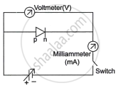
Fig. (a)
Reverse biasing:
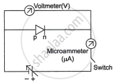
Fig. (b)

Fig. (c)
Figures (a) and (b) depict the circuit for examining a diode's V-I properties. The value of current is noted for various voltage values. The result is a graph between C and I, as shown in Fig. (c).
It is evident from a junction diode's V-I characteristics that current can only flow through it when it is forward biassed. As a result, when alternating voltage is placed across a forward biassed diode, current only flows during a portion of the cycle. Alternating voltages are rectified using this characteristic.
APPEARS IN
संबंधित प्रश्न
Draw a labelled diagram of a full wave rectifier. Show how output voltage varies with time if the input voltage is a sinusoidal voltage.
The graph shown in the figure represents a plot of current versus voltage for a given semiconductor. Identify the region, if any, over which the semiconductor has a negative resistance.

We use alloys for making standard resistors because they have ____________.
In forward bias width of potential barrier in a p + n junction diode
On increasing the reverse biases voltage to a large value in a P – N junction diode-current
In the circuit shown in figure, if the diode forward voltage drop is 0.3 V, the voltage difference between A and B is ______.

Draw V-I characteristics of a p-n Junction diode.
Describe the following term briefly:
Breakdown voltage in reverse biasing
With reference to a semiconductor diode, define the potential barrier.
What is meant by forward biasing of a semiconductor diode?
