Advertisements
Advertisements
प्रश्न
Draw the circuit arrangement for studying V-I characteristics of a p-n junction diode in (i) forward biasing and (ii) reverse biasing. Draw the typical V-I characteristics of a silicon diode.
Advertisements
उत्तर
Forward biasing:
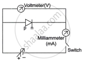
Fig. (a)
Reverse biasing:
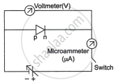
Fig. (b)

Fig. (c)
Figures (a) and (b) depict the circuit for examining a diode's V-I properties. The value of current is noted for various voltage values. The result is a graph between C and I, as shown in Fig. (c).
It is evident from a junction diode's V-I characteristics that current can only flow through it when it is forward biassed. As a result, when alternating voltage is placed across a forward biassed diode, current only flows during a portion of the cycle. Alternating voltages are rectified using this characteristic.
APPEARS IN
संबंधित प्रश्न
Explain the working of P-N junction diode in forward and reverse biased mode.
Basic materials used in the present solid state electronic devices like diode, transistor, ICs, etc are ______.
The drift current in a p-n junction is from the ______.
Consider an npn transistor with its base-emitter junction forward biased and collector base junction reverse biased. Which of the following statements are true?
- Electrons crossover from emitter to collector.
- Holes move from base to collector.
- Electrons move from emitter to base.
- Electrons from emitter move out of base without going to the collector.
The breakdown in a reverse biased p–n junction diode is more likely to occur due to ______.
- large velocity of the minority charge carriers if the doping concentration is small.
- large velocity of the minority charge carriers if the doping concentration is large.
- strong electric field in a depletion region if the doping concentration is small.
- strong electric field in the depletion region if the doping concentration is large.
In the circuit shown in figure, when the input voltage of the base resistance is 10 V, Vbe is zero and Vce is also zero. Find the values of Ib, Ic and β.

Explain the formation of the barrier potential in a p-n junction.
With reference to a semiconductor diode, define the depletion region.
What is meant by forward biasing of a semiconductor diode?
Draw a labelled characteristic curve (l-V graph) for a semiconductor diode during forward bias.
