Advertisements
Advertisements
प्रश्न
The breakdown in a reverse biased p–n junction diode is more likely to occur due to ______.
- large velocity of the minority charge carriers if the doping concentration is small.
- large velocity of the minority charge carriers if the doping concentration is large.
- strong electric field in a depletion region if the doping concentration is small.
- strong electric field in the depletion region if the doping concentration is large.
पर्याय
a and d
b and d
c and d
b and c
Advertisements
उत्तर
a and d
Explanation:
Reverse biasing: Positive terminal of the battery is connected to the N-crystal and negative terminal of the battery is connected to P-crystal.
(i) In reverse biasing width of the depletion layer increases
(ii) In reverse biasing resistance offered `R_("Reverse")` = 105 Ω
(iii) Reverse bias supports the potential barrier and no current flows across the junction due to the diffusion of the majority carriers.
(A very small reverse current may exist in the circuit due to the drifting of minority carriers across the junction)
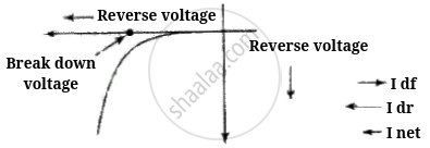
(iv) Break down voltage: Reverse voltage at which break down of semiconductor occurs. For Ge, it is 25 V and for Si, it is 35 V.
So, we conclude that in reverse biasing, ionization takes place because the minority charge carriers will be accelerated due to reverse biasing and striking with atoms which in turn cause secondary electrons and thus more charge carriers.
When doping concentration is large, there will be a large number of ions in the depletion region, which will give rise to a strong electric field.
APPEARS IN
संबंधित प्रश्न
Draw a labelled diagram of a full wave rectifier. Show how output voltage varies with time if the input voltage is a sinusoidal voltage.
Plot a graph showing variation of current versus voltage for the material GaAs ?
Why is a zener diode considered as a special purpose semiconductor diode?
A triode value operates at Vp = 225 V and Vg = −0.5 V.
The plate current remains unchanged if the plate voltage is increased to 250 V and the grid voltage is decreased to −2.5 V. Calculate the amplification factor.
Find the values of rp, µ and gm of a triode operating at plate voltage 200 V and grid voltage −6. The plate characteristics are shown in the figure.

Diffusion in a p-n junction is due to ______.
We use alloys for making standard resistors because they have ____________.
The current through an ideal PN-junction shown in the following circuit diagram will be:

A – pn junction has a depletion layer of thickness .of the order of
When we apply reverse biased to a junction diode, it
In the circuit shown in figure, if the diode forward voltage drop is 0.3 V, the voltage difference between A and B is ______.

Consider an npn transistor with its base-emitter junction forward biased and collector base junction reverse biased. Which of the following statements are true?
- Electrons crossover from emitter to collector.
- Holes move from base to collector.
- Electrons move from emitter to base.
- Electrons from emitter move out of base without going to the collector.
 (a) |
 (b) |
- Name the type of a diode whose characteristics are shown in figure (A) and figure (B).
- What does the point P in figure (A) represent?
- What does the points P and Q in figure (B) represent?
A Zener of power rating 1 W is to be used as a voltage regulator. If zener has a breakdown of 5 V and it has to regulate voltage which fluctuated between 3 V and 7 V, what should be the value of Rs for safe operation (Figure)?

Write the property of a junction diode which makes it suitable for rectification of ac voltages.
A semiconductor device is connected in series with a battery, an ammeter and a resistor. A current flows in the circuit. If. the polarity of the battery is reversed, the current in the circuit almost becomes zero. The device is a/an ______.
Describe the following term briefly:
Breakdown voltage in reverse biasing
With reference to a semiconductor diode, define the depletion region.
A full wave rectifier circuit diodes (D1) and (D2) is shown in the figure. If input supply voltage Vin = 220 sin (100 πt) volt, then at t = 15 ms.

Choose the correct circuit which can achieve the bridge balance.
