Advertisements
Advertisements
प्रश्न
Describe the following term briefly:
Minority carrier injection in forward biasing.
Explain the following term:
Minority carrier injection in forward bias
Advertisements
उत्तर
Due to the applied voltage, electrons from the n-side cross the depletion region and reach the p-side (where they are minority carriers). Similarly, holes from the p-side cross this junction and reach the n-side (where they are minority carriers). This process under forward bias is known as minority carrier injection.
APPEARS IN
संबंधित प्रश्न
(i) Explain with the help of a diagram the formation of depletion region and barrier potential in a pn junction.
In the following diagram 'S' is a semiconductor. Would you increase or decrease the value of R to keep the reading of the ammeter A constant when S is heated? Give reason for your answer.
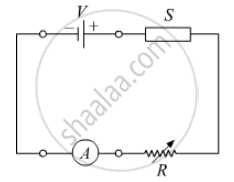
In the following diagram, is the junction diode forward biased or reverse biased ?
With reference to a semiconductor diode, what is meant by:
(i) Forward bias
(ii) Reverse bias
(iii) Depletion region
Avalanche breakdown is due to ______.
Consider an npn transistor with its base-emitter junction forward biased and collector base junction reverse biased. Which of the following statements are true?
- Electrons crossover from emitter to collector.
- Holes move from base to collector.
- Electrons move from emitter to base.
- Electrons from emitter move out of base without going to the collector.
In the depletion region of a diode ______.
- there are no mobile charges.
- equal number of holes and electrons exist, making the region neutral.
- recombination of holes and electrons has taken place.
- immobile charged ions exist.
The breakdown in a reverse biased p–n junction diode is more likely to occur due to ______.
- large velocity of the minority charge carriers if the doping concentration is small.
- large velocity of the minority charge carriers if the doping concentration is large.
- strong electric field in a depletion region if the doping concentration is small.
- strong electric field in the depletion region if the doping concentration is large.
A full wave rectifier circuit diodes (D1) and (D2) is shown in the figure. If input supply voltage Vin = 220 sin (100 πt) volt, then at t = 15 ms.
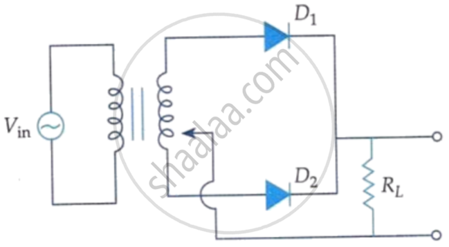
Which formula gives the forward dynamic (AC) resistance?
