Advertisements
Advertisements
Question
The breakdown in a reverse biased p–n junction diode is more likely to occur due to ______.
- large velocity of the minority charge carriers if the doping concentration is small.
- large velocity of the minority charge carriers if the doping concentration is large.
- strong electric field in a depletion region if the doping concentration is small.
- strong electric field in the depletion region if the doping concentration is large.
Options
a and d
b and d
c and d
b and c
Advertisements
Solution
a and d
Explanation:
Reverse biasing: Positive terminal of the battery is connected to the N-crystal and negative terminal of the battery is connected to P-crystal.
(i) In reverse biasing width of the depletion layer increases
(ii) In reverse biasing resistance offered `R_("Reverse")` = 105 Ω
(iii) Reverse bias supports the potential barrier and no current flows across the junction due to the diffusion of the majority carriers.
(A very small reverse current may exist in the circuit due to the drifting of minority carriers across the junction)
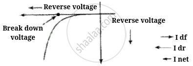
(iv) Break down voltage: Reverse voltage at which break down of semiconductor occurs. For Ge, it is 25 V and for Si, it is 35 V.
So, we conclude that in reverse biasing, ionization takes place because the minority charge carriers will be accelerated due to reverse biasing and striking with atoms which in turn cause secondary electrons and thus more charge carriers.
When doping concentration is large, there will be a large number of ions in the depletion region, which will give rise to a strong electric field.
APPEARS IN
RELATED QUESTIONS
With the help of neat labelled circuit diagram explain the working of half wave rectifier using semiconductor diode. Draw the input and output waveforms.
What happens when a forward bias is applied to a p-n junction?
With reference to semiconductor devices, define a p-type semiconductor and a Zener diode.
Draw a labelled diagram of a full wave rectifier. Show how output voltage varies with time if the input voltage is a sinusoidal voltage.
Show on a graph, the variation of resistivity with temperature for a typical semiconductor.
With reference to semi-conductors answer the following :
(i) What is the change in the resistance of the semi-conductor with increase in temperature ?
(ii) Name the majority charge carriers in n-type semi-conductor.
(iii) What is meant by doping ?
Answer the following question.
Why photodiodes are required to operate in reverse bias? Explain.
We use alloys for making standard resistors because they have ____________.
Depletion layer in p - n junction diode consists of
In forward bias width of potential barrier in a p + n junction diode
Consider an npn transistor with its base-emitter junction forward biased and collector base junction reverse biased. Which of the following statements are true?
- Electrons crossover from emitter to collector.
- Holes move from base to collector.
- Electrons move from emitter to base.
- Electrons from emitter move out of base without going to the collector.
In the depletion region of a diode ______.
- there are no mobile charges.
- equal number of holes and electrons exist, making the region neutral.
- recombination of holes and electrons has taken place.
- immobile charged ions exist.
A Zener of power rating 1 W is to be used as a voltage regulator. If zener has a breakdown of 5 V and it has to regulate voltage which fluctuated between 3 V and 7 V, what should be the value of Rs for safe operation (Figure)?

The graph of potential barrier versus width of depletion region for an unbiased diode is shown in graph A. In comparison to A, graphs B and C are obtained after biasing the diode in different ways. Identify the type of biasing in B and C and justify your answer
| ‘A’ | ‘B’ | ‘C’ |
 |
 |
 |
Draw V-I characteristics of a p-n Junction diode.
Differentiate between the threshold voltage and the breakdown voltage for a diode.
Explain the formation of the barrier potential in a p-n junction.
Draw the circuit arrangement for studying V-I characteristics of a p-n junction diode in (i) forward biasing and (ii) reverse biasing. Draw the typical V-I characteristics of a silicon diode.
Describe the following term briefly:
Breakdown voltage in reverse biasing
With reference to a semiconductor diode, define the potential barrier.
