Advertisements
Advertisements
Question
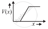
The graph of potential barrier versus width of depletion region for an unbiased diode is shown in graph A. In comparison to A, graphs B and C are obtained after biasing the diode in different ways. Identify the type of biasing in B and C and justify your answer
| ‘A’ | ‘B’ | ‘C’ |
 |
 |
 |
Advertisements
Solution
B - reverse biased
In the case of a reverse-biased diode, the potential barrier becomes higher as the battery further raises the potential of the n side.
C - forward biased
Due to the forward bias connection, the potential of P side is raised and hence the height of the potential barrier decreases.
APPEARS IN
RELATED QUESTIONS
(i) Explain with the help of a diagram the formation of depletion region and barrier potential in a pn junction.
With reference to semiconductor devices, define a p-type semiconductor and a Zener diode.
The graph shown in the figure represents a plot of current versus voltage for a given semiconductor. Identify the region, if any, over which the semiconductor has a negative resistance.

The current through an ideal PN-junction shown in the following circuit diagram will be:

When we apply reverse biased to a junction diode, it
A Zener of power rating 1 W is to be used as a voltage regulator. If zener has a breakdown of 5 V and it has to regulate voltage which fluctuated between 3 V and 7 V, what should be the value of Rs for safe operation (Figure)?

Describe the following term briefly:
Breakdown voltage in reverse biasing
What is meant by forward biasing of a semiconductor diode?
How does effective resistance compare between forward bias after the cut-in voltage and reverse bias before breakdown?
Which formula gives the forward dynamic (AC) resistance?
