Advertisements
Advertisements
Question
A plate current of 10 mA is obtained when 60 volts are applied across a diode tube. Assuming the Langmuir-Child relation \[i_p \infty V_p^{3/2}\] to hold, find the dynamic resistance rp in this operating condition.
Advertisements
Solution
According to Lamgmuir-Child Law,
the relation between plate current (ip) and the plate voltage (Vp) is given by
\[i_p = C {V_p}^{3/2} ............(1)\]
Differentiating equation (1) with respect Vp, we get:-
\[\frac{d i_p}{d V_p} = \frac{3}{2}C {V_p}^{1/2} ............(2)\]
Dividing (2) and (1), we get:-
\[\frac{1}{i_p}\frac{d i_p}{d v_p} = \frac{3/2C {V_p}^{1/2}}{C {V_p}^{3/2}}\]
\[ \Rightarrow \frac{1}{i_p} . \frac{d i_p}{d v_p} = \frac{3}{2 V_p}\]
The dynamic resistance is given by:-
\[\frac{d v_p}{d i_p} = \frac{2 V_p}{3 i_p}\]
\[ r_p = \frac{2 V_p}{3 i_p}\]
\[ r_p = \frac{2 \times 60}{3 \times 10 \times {10}^{- 3}}\]
\[ r_p = 4 \times {10}^3 = 4 k\Omega\]
APPEARS IN
RELATED QUESTIONS
With the help of neat labelled circuit diagram explain the working of half wave rectifier using semiconductor diode. Draw the input and output waveforms.
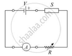
In the following diagram 'S' is a semiconductor. Would you increase or decrease the value of R to keep the reading of the ammeter A constant when S is heated? Give reason for your answer.
With reference to semiconductor devices, define a p-type semiconductor and a Zener diode.
Draw a labelled diagram of a full wave rectifier. Show how output voltage varies with time if the input voltage is a sinusoidal voltage.
The graph shown in the figure represents a plot of current versus voltage for a given semiconductor. Identify the region, if any, over which the semiconductor has a negative resistance.

With reference to semi-conductors answer the following :
(i) What is the change in the resistance of the semi-conductor with increase in temperature ?
(ii) Name the majority charge carriers in n-type semi-conductor.
(iii) What is meant by doping ?
The dynamic plate resistance of a triode value is 10 kΩ. Find the change in the plate current if the plate voltage is changed from 200 V to 220 V.
In semiconductor physics, what is meant by:
(i) rectifier
(ii) an amplifier
(iii) an oscillator
The current through an ideal PN-junction shown in the following circuit diagram will be:

The expected energy of the electron at absolute zero is called:-
In Figure, Vo is the potential barrier across a p-n junction, when no battery is connected across the junction ______.

Consider an npn transistor with its base-emitter junction forward biased and collector base junction reverse biased. Which of the following statements are true?
- Electrons crossover from emitter to collector.
- Holes move from base to collector.
- Electrons move from emitter to base.
- Electrons from emitter move out of base without going to the collector.
If each diode in figure has a forward bias resistance of 25 Ω and infinite resistance in reverse bias, what will be the values of the current I1, I2, I3 and I4?

Draw V-I characteristics of a p-n Junction diode.
Explain the formation of the barrier potential in a p-n junction.
Draw the circuit arrangement for studying V-I characteristics of a p-n junction diode in (i) forward biasing and (ii) reverse biasing. Draw the typical V-I characteristics of a silicon diode.
Describe the following term briefly:
Minority carrier injection in forward biasing.
Describe the following term briefly:
Breakdown voltage in reverse biasing
Draw a labelled characteristic curve (l-V graph) for a semiconductor diode during forward bias.
