Advertisements
Advertisements
Questions
Write the property of a junction diode which makes it suitable for rectification of ac voltages.
Which characteristic property makes the junction diode suitable for rectification?
State the characteristic property of a junction diode that makes it suitable for rectification.
Advertisements
Solution
When a junction diode has an alternating voltage placed across it, only when the diode is forward-biased can current flow. The junction diode's ability to correct alternating current can be used. This is accomplished through the use of a rectifier circuit. It exhibits high resistance when reverse-biased and low resistance when forward-biased.
APPEARS IN
RELATED QUESTIONS
(i) Explain with the help of a diagram the formation of depletion region and barrier potential in a pn junction.
With the help of neat labelled circuit diagram explain the working of half wave rectifier using semiconductor diode. Draw the input and output waveforms.
Draw its I – V characteristics of photodiode
The plate current in a diode is 20 mA when the plate voltage is 50 V or 60 V. What will be the current if the plate voltage is 70 V?
The power delivered in the plate circular of a diode is 1.0 W when the plate voltage is 36 V. Find the power delivered if the plate voltage is increased to 49 V. Assume Langmuir-Child equation to hold.
On increasing the reverse biases voltage to a large value in a P – N junction diode-current
In Figure, Vo is the potential barrier across a p-n junction, when no battery is connected across the junction ______.

Consider a box with three terminals on top of it as shown in figure (a):
 (a) |
Three components namely, two germanium diodes and one resistor are connected across these three terminals in some arrangement. A student performs an experiment in which any two of these three terminals are connected in the circuit shown in figure (b).
 (b) |
The student obtains graphs of current-voltage characteristics for unknown combination of components between the two terminals connected in the circuit. The graphs are
(i) when A is positive and B is negative
 (c) |
(ii) when A is negative and B is positive
 (d) |
(iii) When B is negative and C is positive
|
(e) |

(iv) When B is positive and C is negative
 (f) |
(v) When A is positive and C is negative
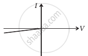 (g) |
(vi) When A is negative and C is positive
 (h) |
From these graphs of current-voltage characteristics shown in figure (c) to (h), determine the arrangement of components between A, B and C.
Draw a labelled characteristic curve (l-V graph) for a semiconductor diode during forward bias.
What is the approximate cut-in voltage of a silicon diode?
