Advertisements
Advertisements
Question
Draw the circuit arrangement for studying V-I characteristics of a p-n junction diode in (i) forward biasing and (ii) reverse biasing. Draw the typical V-I characteristics of a silicon diode.
Advertisements
Solution
Forward biasing:
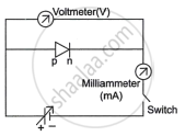
Fig. (a)
Reverse biasing:
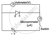
Fig. (b)

Fig. (c)
Figures (a) and (b) depict the circuit for examining a diode's V-I properties. The value of current is noted for various voltage values. The result is a graph between C and I, as shown in Fig. (c).
It is evident from a junction diode's V-I characteristics that current can only flow through it when it is forward biassed. As a result, when alternating voltage is placed across a forward biassed diode, current only flows during a portion of the cycle. Alternating voltages are rectified using this characteristic.
APPEARS IN
RELATED QUESTIONS
(i) Explain with the help of a diagram the formation of depletion region and barrier potential in a pn junction.
With the help of neat labelled circuit diagram explain the working of half wave rectifier using semiconductor diode. Draw the input and output waveforms.
Draw a labelled diagram of a full wave rectifier. Show how output voltage varies with time if the input voltage is a sinusoidal voltage.
Diffusion in a p-n junction is due to ______.
We use alloys for making standard resistors because they have ____________.
The nature of binding for a crystal with alternate and evenly spaced positive and negatively ions is
In forward bias width of potential barrier in a p + n junction diode
The graph of potential barrier versus width of depletion region for an unbiased diode is shown in graph A. In comparison to A, graphs B and C are obtained after biasing the diode in different ways. Identify the type of biasing in B and C and justify your answer
| ‘A’ | ‘B’ | ‘C’ |
 |
 |
 |
A semiconductor device is connected in series with a battery, an ammeter and a resistor. A current flows in the circuit. If. the polarity of the battery is reversed, the current in the circuit almost becomes zero. The device is a/an ______.
Describe the following term briefly:
minority carrier injection in forward biasing.
