Advertisements
Advertisements
Question
Explain the working of P-N junction diode in forward and reverse biased mode.
Advertisements
Solution
If a germanium crystal or silicon crystal is doped during manufacture in such a way that half of it is p-type and other half is n-type, we get p-n junction.
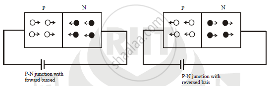
(a) Forward biased: A battery is connected across p-n junction diode such that, p-type is connected to positive terminal and n-type is connected to negative terminal, then it is called forward biased. The potential difference applied should be more than 0.3 V for germanium and more than 0.7 V for silicon. Then holes from p-type region and electrons from n-type region moves towards barrier and it decreases width and height of
barrier. Hence an electric current flows through circuit. When applied potential is zero, then current also equal to zero. When P.D. Increases the current is also increases but very slowly. When applied P.D. is more than potential barrier, current in creases rapidly. This voltage is called knee voltage. The forward biased voltage at which the current through diode increases rapidly is called knee voltage
b) Reversed biased : A battery is connected across p-n junction diode such that, p-type is connected to negative terminal and n-type is connected to positive terminal, then it is called reversed biased. The holes from p type region and electrons from n-type region moves away from junction and it increases width and height of barrier. Hence there is no flow of an electric current in ideal case. In actual case current is very small (inμA) . The width of potential barrier increases and diode offer very high resistance. The very small current flows through circuit is called as reverse current. If reversed bias voltage increased then the kinetic energy of electrons increases. At certain reversed bias voltage the K.E. of electrons increases enough and they knock out the electrons from semiconductor atoms\ Therefore current suddenly increase. That certain reversed bias voltage is called as breakdown voltage. At breakdown voltage the current increases suddenly and destroy the junction permanently. The reversed bas voltage at which P-N junction breaks and current suddenly increases is called as breakdown voltage.
APPEARS IN
RELATED QUESTIONS
(i) Explain with the help of a diagram the formation of depletion region and barrier potential in a pn junction.
What happens when a forward bias is applied to a p-n junction?
What causes the setting up of high electric field even for small reverse bias voltage across the diode?
In the following diagram 'S' is a semiconductor. Would you increase or decrease the value of R to keep the reading of the ammeter A constant when S is heated? Give reason for your answer.
In the following diagram, is the junction diode forward biased or reverse biased ?
What is the use of Zener diode?
Draw a labelled diagram of a full wave rectifier. Show how output voltage varies with time if the input voltage is a sinusoidal voltage.
With reference to semi-conductors answer the following :
(i) What is the change in the resistance of the semi-conductor with increase in temperature ?
(ii) Name the majority charge carriers in n-type semi-conductor.
(iii) What is meant by doping ?
A plate current of 10 mA is obtained when 60 volts are applied across a diode tube. Assuming the Langmuir-Child relation \[i_p \infty V_p^{3/2}\] to hold, find the dynamic resistance rp in this operating condition.
The power delivered in the plate circular of a diode is 1.0 W when the plate voltage is 36 V. Find the power delivered if the plate voltage is increased to 49 V. Assume Langmuir-Child equation to hold.
The gain factor of an amplifier in increased from 10 to 12 as the load resistance is changed from 4 kΩ to 8 kΩ. Calculate (a) the amplification factor and (b) the plate resistance.
With reference to a semiconductor diode, what is meant by:
(i) Forward bias
(ii) Reverse bias
(iii) Depletion region
In semiconductor physics, what is meant by:
(i) rectifier
(ii) an amplifier
(iii) an oscillator
We use alloys for making standard resistors because they have ____________.
What are the applications of p - n Junction diode?
Of the diodes shown in the following diagrams, which one is reverse biased?
The drift current in a p-n junction is from the ______.
The nature of binding for a crystal with alternate and evenly spaced positive and negatively ions is
Consider an npn transistor with its base-emitter junction forward biased and collector base junction reverse biased. Which of the following statements are true?
- Electrons crossover from emitter to collector.
- Holes move from base to collector.
- Electrons move from emitter to base.
- Electrons from emitter move out of base without going to the collector.
In the depletion region of a diode ______.
- there are no mobile charges.
- equal number of holes and electrons exist, making the region neutral.
- recombination of holes and electrons has taken place.
- immobile charged ions exist.
The breakdown in a reverse biased p–n junction diode is more likely to occur due to ______.
- large velocity of the minority charge carriers if the doping concentration is small.
- large velocity of the minority charge carriers if the doping concentration is large.
- strong electric field in a depletion region if the doping concentration is small.
- strong electric field in the depletion region if the doping concentration is large.
Consider a box with three terminals on top of it as shown in figure (a):
 (a) |
Three components namely, two germanium diodes and one resistor are connected across these three terminals in some arrangement. A student performs an experiment in which any two of these three terminals are connected in the circuit shown in figure (b).
 (b) |
The student obtains graphs of current-voltage characteristics for unknown combination of components between the two terminals connected in the circuit. The graphs are
(i) when A is positive and B is negative
 (c) |
(ii) when A is negative and B is positive
 (d) |
(iii) When B is negative and C is positive
|
(e) |

(iv) When B is positive and C is negative
 (f) |
(v) When A is positive and C is negative
 (g) |
(vi) When A is negative and C is positive
 (h) |
From these graphs of current-voltage characteristics shown in figure (c) to (h), determine the arrangement of components between A, B and C.
A semiconductor device is connected in series with a battery, an ammeter and a resistor. A current flows in the circuit. If. the polarity of the battery is reversed, the current in the circuit almost becomes zero. The device is a/an ______.
With reference to a semiconductor diode, define the potential barrier.
What is meant by forward biasing of a semiconductor diode?
An ideal PN junction diode offers ______.
Choose the correct circuit which can achieve the bridge balance.
