Advertisements
Advertisements
Question
Find the values of rp, µ and gm of a triode operating at plate voltage 200 V and grid voltage −6. The plate characteristics are shown in the figure.

Advertisements
Solution
Dynamic plate resistance, `r_p=((deltaV_p)/(deltaI_p)),` at constant grid voltage
We need to find the slope of the graph for a particular value of grid voltage, i.e. Vg = −6 V.
Consider two points for the plot of Vg = −6 V:-
\[r_p = \frac{(240 - 160) V}{(13 - 3) \times {10}^{- 3} A}\]
\[ r_p = \frac{80}{10} \times {10}^3 \Omega\]
\[ r_p = 8 K\Omega\]
\[ g_m = \left( \frac{\delta I_p}{\delta V_g} \right)_{V_P = \text{constant } (200 V)}\]
Consider two points on the 200 V line:-
\[g_m = \frac{(13 - 3) \times {10}^{- 3}}{[( - 4) - ( - 8)]}A\]
\[ g_m = \frac{10 \times {10}^{- 3}}{4}=2.5\text{ mili mho}\]
Amplification factor,
\[\mu = - \left( \frac{∆ V_P}{∆ V_G} \right)_{i_P =\text{ constant}}\]
\[\mu = - \frac{100 - 180}{- 6 - ( - 10)}\]
\[\mu = \frac{80}{4} = 20\]
APPEARS IN
RELATED QUESTIONS
What happens when a forward bias is applied to a p-n junction?
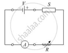
In the following diagram 'S' is a semiconductor. Would you increase or decrease the value of R to keep the reading of the ammeter A constant when S is heated? Give reason for your answer.
Draw its I – V characteristics of photodiode
In the following diagram, is the junction diode forward biased or reverse biased ?
With reference to semiconductor devices, define a p-type semiconductor and a Zener diode.
What is the use of Zener diode?
In a photo diode, the conductive increases when the material is exposed to light. It is found that the conductivity changes only if the wavelength is less than 620 nm. What is the band gap?
(Use Planck constant h = 4.14 × 10⁻¹⁵ eV-s, Boltzmann constant k = 8·62 × 10-5 eV/K.)
A triode value operates at Vp = 225 V and Vg = −0.5 V.
The plate current remains unchanged if the plate voltage is increased to 250 V and the grid voltage is decreased to −2.5 V. Calculate the amplification factor.
The gain factor of an amplifier in increased from 10 to 12 as the load resistance is changed from 4 kΩ to 8 kΩ. Calculate (a) the amplification factor and (b) the plate resistance.
What are the applications of p - n Junction diode?
The current through an ideal PN-junction shown in the following circuit diagram will be:

A – pn junction has a depletion layer of thickness .of the order of
When we apply reverse biased to a junction diode, it
Can the potential barrier across a p-n junction be measured by simply connecting a voltmeter across the junction?
A Zener of power rating 1 W is to be used as a voltage regulator. If zener has a breakdown of 5 V and it has to regulate voltage which fluctuated between 3 V and 7 V, what should be the value of Rs for safe operation (Figure)?

If each diode in figure has a forward bias resistance of 25 Ω and infinite resistance in reverse bias, what will be the values of the current I1, I2, I3 and I4?

With reference to a semiconductor diode, define the depletion region.
