Advertisements
Advertisements
प्रश्न
Find the values of rp, µ and gm of a triode operating at plate voltage 200 V and grid voltage −6. The plate characteristics are shown in the figure.

Advertisements
उत्तर
Dynamic plate resistance, `r_p=((deltaV_p)/(deltaI_p)),` at constant grid voltage
We need to find the slope of the graph for a particular value of grid voltage, i.e. Vg = −6 V.
Consider two points for the plot of Vg = −6 V:-
\[r_p = \frac{(240 - 160) V}{(13 - 3) \times {10}^{- 3} A}\]
\[ r_p = \frac{80}{10} \times {10}^3 \Omega\]
\[ r_p = 8 K\Omega\]
\[ g_m = \left( \frac{\delta I_p}{\delta V_g} \right)_{V_P = \text{constant } (200 V)}\]
Consider two points on the 200 V line:-
\[g_m = \frac{(13 - 3) \times {10}^{- 3}}{[( - 4) - ( - 8)]}A\]
\[ g_m = \frac{10 \times {10}^{- 3}}{4}=2.5\text{ mili mho}\]
Amplification factor,
\[\mu = - \left( \frac{∆ V_P}{∆ V_G} \right)_{i_P =\text{ constant}}\]
\[\mu = - \frac{100 - 180}{- 6 - ( - 10)}\]
\[\mu = \frac{80}{4} = 20\]
APPEARS IN
संबंधित प्रश्न
(i) Explain with the help of a diagram the formation of depletion region and barrier potential in a pn junction.
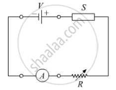
In the following diagram 'S' is a semiconductor. Would you increase or decrease the value of R to keep the reading of the ammeter A constant when S is heated? Give reason for your answer.
Draw its I – V characteristics of photodiode
In the following diagram, is the junction diode forward biased or reverse biased ?
With reference to semiconductor devices, define a p-type semiconductor and a Zener diode.
The graph shown in the figure represents a plot of current versus voltage for a given semiconductor. Identify the region, if any, over which the semiconductor has a negative resistance.

Show on a graph, the variation of resistivity with temperature for a typical semiconductor.
With reference to semi-conductors answer the following :
(i) What is the change in the resistance of the semi-conductor with increase in temperature ?
(ii) Name the majority charge carriers in n-type semi-conductor.
(iii) What is meant by doping ?
A plate current of 10 mA is obtained when 60 volts are applied across a diode tube. Assuming the Langmuir-Child relation \[i_p \infty V_p^{3/2}\] to hold, find the dynamic resistance rp in this operating condition.
A triode value operates at Vp = 225 V and Vg = −0.5 V.
The plate current remains unchanged if the plate voltage is increased to 250 V and the grid voltage is decreased to −2.5 V. Calculate the amplification factor.
The gain factor of an amplifier in increased from 10 to 12 as the load resistance is changed from 4 kΩ to 8 kΩ. Calculate (a) the amplification factor and (b) the plate resistance.
In semiconductor physics, what is meant by:
(i) rectifier
(ii) an amplifier
(iii) an oscillator
Diffusion in a p-n junction is due to ______.
When we apply reverse biased to a junction diode, it
In forward bias width of potential barrier in a p + n junction diode
Consider a box with three terminals on top of it as shown in figure (a):
 (a) |
Three components namely, two germanium diodes and one resistor are connected across these three terminals in some arrangement. A student performs an experiment in which any two of these three terminals are connected in the circuit shown in figure (b).
 (b) |
The student obtains graphs of current-voltage characteristics for unknown combination of components between the two terminals connected in the circuit. The graphs are
(i) when A is positive and B is negative
 (c) |
(ii) when A is negative and B is positive
 (d) |
(iii) When B is negative and C is positive
|
(e) |

(iv) When B is positive and C is negative
 (f) |
(v) When A is positive and C is negative
 (g) |
(vi) When A is negative and C is positive
 (h) |
From these graphs of current-voltage characteristics shown in figure (c) to (h), determine the arrangement of components between A, B and C.
A semiconductor device is connected in series with a battery, an ammeter and a resistor. A current flows in the circuit. If. the polarity of the battery is reversed, the current in the circuit almost becomes zero. The device is a/an ______.
Describe the following term briefly:
Minority carrier injection in forward biasing.
With reference to a semiconductor diode, define the depletion region.
An ideal PN junction diode offers ______.
