Advertisements
Advertisements
प्रश्न
Can the potential barrier across a p-n junction be measured by simply connecting a voltmeter across the junction?
Advertisements
उत्तर
We cannot measure the potential barrier across a p-n junction by a voltmeter because the resistance of the voltmeter is very high compared to the junction resistance. Potential of potential barrier for Ge is VB = 0.3 V and for silicon is VB = 0.7 V.
On average the potential barrier in the P-N junction is ~0.5 V.
APPEARS IN
संबंधित प्रश्न
When a forward bias is applied to a p-n junction, it ______.
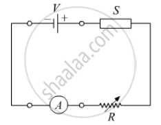
In the following diagram 'S' is a semiconductor. Would you increase or decrease the value of R to keep the reading of the ammeter A constant when S is heated? Give reason for your answer.
Draw its I – V characteristics of photodiode
Show on a graph, the variation of resistivity with temperature for a typical semiconductor.
Why is a zener diode considered as a special purpose semiconductor diode?
The plate current in a diode is 20 mA when the plate voltage is 50 V or 60 V. What will be the current if the plate voltage is 70 V?
With reference to a semiconductor diode, what is meant by:
(i) Forward bias
(ii) Reverse bias
(iii) Depletion region
With reference to Semiconductor Physics,
Name the diode that emits spontaneous radiation when forward biased.
What are the applications of p - n Junction diode?
The drift current in a p-n junction is from the ______.
In forward bias width of potential barrier in a p + n junction diode
Use a transistor as an amplition
In Figure, Vo is the potential barrier across a p-n junction, when no battery is connected across the junction ______.

Consider an npn transistor with its base-emitter junction forward biased and collector base junction reverse biased. Which of the following statements are true?
- Electrons crossover from emitter to collector.
- Holes move from base to collector.
- Electrons move from emitter to base.
- Electrons from emitter move out of base without going to the collector.
The breakdown in a reverse biased p–n junction diode is more likely to occur due to ______.
- large velocity of the minority charge carriers if the doping concentration is small.
- large velocity of the minority charge carriers if the doping concentration is large.
- strong electric field in a depletion region if the doping concentration is small.
- strong electric field in the depletion region if the doping concentration is large.
Draw the circuit arrangement for studying V-I characteristics of a p-n junction diode in (i) forward biasing and (ii) reverse biasing. Draw the typical V-I characteristics of a silicon diode.
Draw a labelled characteristic curve (l-V graph) for a semiconductor diode during forward bias.
Choose the correct circuit which can achieve the bridge balance.
