Advertisements
Advertisements
प्रश्न
Can the potential barrier across a p-n junction be measured by simply connecting a voltmeter across the junction?
Advertisements
उत्तर
We cannot measure the potential barrier across a p-n junction by a voltmeter because the resistance of the voltmeter is very high compared to the junction resistance. Potential of potential barrier for Ge is VB = 0.3 V and for silicon is VB = 0.7 V.
On average the potential barrier in the P-N junction is ~0.5 V.
APPEARS IN
संबंधित प्रश्न
Explain the working of P-N junction diode in forward and reverse biased mode.
In the following diagram, is the junction diode forward biased or reverse biased ?
Basic materials used in the present solid state electronic devices like diode, transistor, ICs, etc are ______.
With reference to Semiconductor Physics,
Name the diode that emits spontaneous radiation when forward biased.
Of the diodes shown in the following diagrams, which one is reverse biased?
The current through an ideal PN-junction shown in the following circuit diagram will be:

Depletion layer in p - n junction diode consists of
Consider an npn transistor with its base-emitter junction forward biased and collector base junction reverse biased. Which of the following statements are true?
- Electrons crossover from emitter to collector.
- Holes move from base to collector.
- Electrons move from emitter to base.
- Electrons from emitter move out of base without going to the collector.
Consider a box with three terminals on top of it as shown in figure (a):
 (a) |
Three components namely, two germanium diodes and one resistor are connected across these three terminals in some arrangement. A student performs an experiment in which any two of these three terminals are connected in the circuit shown in figure (b).
 (b) |
The student obtains graphs of current-voltage characteristics for unknown combination of components between the two terminals connected in the circuit. The graphs are
(i) when A is positive and B is negative
 (c) |
(ii) when A is negative and B is positive
 (d) |
(iii) When B is negative and C is positive
|
(e) |

(iv) When B is positive and C is negative
 (f) |
(v) When A is positive and C is negative
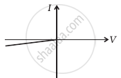 (g) |
(vi) When A is negative and C is positive
 (h) |
From these graphs of current-voltage characteristics shown in figure (c) to (h), determine the arrangement of components between A, B and C.
Explain the formation of the barrier potential in a p-n junction.
Read the following paragraph and answer the questions that follow.
| A semiconductor diode is basically a pn junction with metallic contacts provided at the ends for the application of an external voltage. It is a two-terminal device. When an external voltage is applied across a semiconductor diode such that the p-side is connected to the positive terminal of the battery and the n-side to the negative terminal, it is said to be forward-biased. When an external voltage is applied across the diode such that the n-side is positive and the p-side is negative, it is said to be reverse-biased. An ideal diode is one whose resistance in forward biasing is zero and the resistance is infinite in reverse biasing. When the diode is forward biased, it is found that beyond forward voltage called knee voltage, the conductivity is very high. When the biasing voltage is more than the knee voltage the potential barrier is overcome and the current increases rapidly with an increase in forward voltage. When the diode is reverse biased, the reverse bias voltage produces a very small current of about a few microamperes which almost remains constant with bias. This small current is a reverse saturation current. |
- In the given figure, a diode D is connected to an external resistance R = 100 Ω and an emf of 3.5 V. If the barrier potential developed across the diode is 0.5 V, the current in the circuit will be:
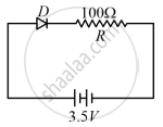
(a) 40 mA
(b) 20 mA
(c) 35 mA
(d) 30 mA - In which of the following figures, the pn diode is reverse biased?
(a)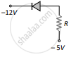
(b)
(c)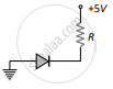
(d)
- Based on the V-I characteristics of the diode, we can classify the diode as:
(a) bilateral device
(b) ohmic device
(c) non-ohmic device
(d) passive element
OR
Two identical PN junctions can be connected in series by three different methods as shown in the figure. If the potential difference in the junctions is the same, then the correct connections will be:
(a) in the circuits (1) and (2)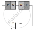

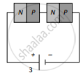
(b) in the circuits (2) and (3)
(c) in the circuits (1) and (3)
(d) only in the circuit (1) 
The V-I characteristic of a diode is shown in the figure. The ratio of the resistance of the diode at I = 15 mA to the resistance at V = -10 V is
(a) 100
(b) 106
(c) 10
(d) 10-6
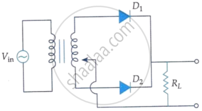
A full wave rectifier circuit diodes (D1) and (D2) is shown in the figure. If input supply voltage Vin = 220 sin (100 πt) volt, then at t = 15 ms.
When the p-side and n-side are joined, in which direction do electrons diffuse?
What is the approximate cut-in voltage of a germanium diode?
Which practical effect is associated with forward bias?
Which voltage corresponds to a forward current of \[10\,\mathrm{mA}\]?
What does the comparison of \[10\,\Omega\] in forward bias and \[1.0\times10^{7}\,\Omega\] in reverse bias show?
