Advertisements
Advertisements
प्रश्न
Consider an npn transistor with its base-emitter junction forward biased and collector base junction reverse biased. Which of the following statements are true?
- Electrons crossover from emitter to collector.
- Holes move from base to collector.
- Electrons move from emitter to base.
- Electrons from emitter move out of base without going to the collector.
विकल्प
d and a
a and b
b and c
a and c
Advertisements
उत्तर
a and c
Explanation:
Transistor: A junction transistor is formed by sandwiching 2 thin layer of P-type semiconductors between two N-type semiconductors. or by sandwiching a thin taver of V-type semiconductors between two P-type semiconductors.
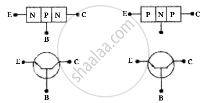
E — Emitter (emits majority charge carriers)
C — Collects majority charge carriers
B — Base (provide proper interaction between E and C)

In normal operation base-emitter is forward biased, i.e., the positive pole of the emitter-base battery is connected to the base and its negative pole is connected to the emitter. And collector-base junction is reverse biased, i.e., the positive pole of the collector base battery is connected to the collector and the negative pole to base. Thus, electron moves from emitter to base and crossovers from emitter to collector.
APPEARS IN
संबंधित प्रश्न
When a forward bias is applied to a p-n junction, it ______.
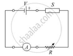
In the following diagram 'S' is a semiconductor. Would you increase or decrease the value of R to keep the reading of the ammeter A constant when S is heated? Give reason for your answer.
With reference to semiconductor devices, define a p-type semiconductor and a Zener diode.
Plot a graph showing variation of current versus voltage for the material GaAs ?
Why is a zener diode considered as a special purpose semiconductor diode?
A triode value operates at Vp = 225 V and Vg = −0.5 V.
The plate current remains unchanged if the plate voltage is increased to 250 V and the grid voltage is decreased to −2.5 V. Calculate the amplification factor.
Find the values of rp, µ and gm of a triode operating at plate voltage 200 V and grid voltage −6. The plate characteristics are shown in the figure.

Basic materials used in the present solid state electronic devices like diode, transistor, ICs, etc are ______.
The drift current in a p-n junction is from the ______.
Use a transistor as an amplition
On increasing the reverse biases voltage to a large value in a P – N junction diode-current
Consider an npn transistor with its base-emitter junction forward biased and collector base junction reverse biased. Which of the following statements are true?
- Electrons crossover from emitter to collector.
- Holes move from base to collector.
- Electrons move from emitter to base.
- Electrons from emitter move out of base without going to the collector.
 (a) |
 (b) |
- Name the type of a diode whose characteristics are shown in figure (A) and figure (B).
- What does the point P in figure (A) represent?
- What does the points P and Q in figure (B) represent?
Consider a box with three terminals on top of it as shown in figure (a):
 (a) |
Three components namely, two germanium diodes and one resistor are connected across these three terminals in some arrangement. A student performs an experiment in which any two of these three terminals are connected in the circuit shown in figure (b).
 (b) |
The student obtains graphs of current-voltage characteristics for unknown combination of components between the two terminals connected in the circuit. The graphs are
(i) when A is positive and B is negative
 (c) |
(ii) when A is negative and B is positive
 (d) |
(iii) When B is negative and C is positive
|
(e) |

(iv) When B is positive and C is negative
 (f) |
(v) When A is positive and C is negative
 (g) |
(vi) When A is negative and C is positive
 (h) |
From these graphs of current-voltage characteristics shown in figure (c) to (h), determine the arrangement of components between A, B and C.
The graph of potential barrier versus width of depletion region for an unbiased diode is shown in graph A. In comparison to A, graphs B and C are obtained after biasing the diode in different ways. Identify the type of biasing in B and C and justify your answer
| ‘A’ | ‘B’ | ‘C’ |
 |
 |
 |
Differentiate between the threshold voltage and the breakdown voltage for a diode.
Describe the following term briefly:
Minority carrier injection in forward biasing.
With reference to a semiconductor diode, define the depletion region.
What is meant by forward biasing of a semiconductor diode?
A full wave rectifier circuit diodes (D1) and (D2) is shown in the figure. If input supply voltage Vin = 220 sin (100 πt) volt, then at t = 15 ms.

