Advertisements
Advertisements
प्रश्न
The gain factor of an amplifier in increased from 10 to 12 as the load resistance is changed from 4 kΩ to 8 kΩ. Calculate (a) the amplification factor and (b) the plate resistance.
Advertisements
उत्तर
We know:-
Voltage gain = \[\frac{\mu}{1 + \frac{r_p}{R_L}} ............(1)\]
When voltage amplification factor, A = 10,
RL = 4 kΩ
\[10 = \frac{\mu}{1 + \frac{r_p}{4 \times {10}^3}}\]
\[\Rightarrow 10=\frac{\mu \times 4 \times {10}^3}{4 \times {10}^3 + r_p}\]
\[ \Rightarrow 4 \times {10}^4 + 10 r_P = 4000 \mu .........(2)\]
Now, increased gain, A = 12
Substituting this value in (1) ,we get:-
\[12 = \frac{\mu}{1 + \frac{r_P}{R_L}}\]
\[12 = \frac{\mu}{1 + \frac{r_p}{8 \times {10}^3}}\]
\[ \Rightarrow 12 = \frac{\mu \times 8000}{8000 + r_P}\]
\[ \Rightarrow 96000 + 12 r_P = 8000 \mu ...........(3)\]
On solving equations (2) and (3), we get:-
\[\mu = 15\]
\[ r_P = 2000 Ω = 2 k\Omega\]
APPEARS IN
संबंधित प्रश्न
With the help of neat labelled circuit diagram explain the working of half wave rectifier using semiconductor diode. Draw the input and output waveforms.
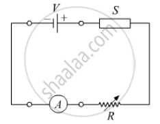
In the following diagram 'S' is a semiconductor. Would you increase or decrease the value of R to keep the reading of the ammeter A constant when S is heated? Give reason for your answer.
The graph shown in the figure represents a plot of current versus voltage for a given semiconductor. Identify the region, if any, over which the semiconductor has a negative resistance.

Show on a graph, the variation of resistivity with temperature for a typical semiconductor.
With reference to semi-conductors answer the following :
(i) What is the change in the resistance of the semi-conductor with increase in temperature ?
(ii) Name the majority charge carriers in n-type semi-conductor.
(iii) What is meant by doping ?
A plate current of 10 mA is obtained when 60 volts are applied across a diode tube. Assuming the Langmuir-Child relation \[i_p \infty V_p^{3/2}\] to hold, find the dynamic resistance rp in this operating condition.
A triode value operates at Vp = 225 V and Vg = −0.5 V.
The plate current remains unchanged if the plate voltage is increased to 250 V and the grid voltage is decreased to −2.5 V. Calculate the amplification factor.
Basic materials used in the present solid state electronic devices like diode, transistor, ICs, etc are ______.
With reference to Semiconductor Physics,
Name the diode that emits spontaneous radiation when forward biased.
The current through an ideal PN-junction shown in the following circuit diagram will be:

The drift current in a p-n junction is from the ______.
When we apply reverse biased to a junction diode, it
Avalanche breakdown is due to ______.
Figure shows the transfer characteristics of a base biased CE transistor. Which of the following statements are true?

At Vi = 0.4 V, transistor is in active state.
At Vi = 1 V, it can be used as an amplifier.
At Vi = 0.5 V, it can be used as a switch turned off.
At Vi = 2.5 V, it can be used as a switch turned on.
In the depletion region of a diode ______.
- there are no mobile charges.
- equal number of holes and electrons exist, making the region neutral.
- recombination of holes and electrons has taken place.
- immobile charged ions exist.
The graph of potential barrier versus width of depletion region for an unbiased diode is shown in graph A. In comparison to A, graphs B and C are obtained after biasing the diode in different ways. Identify the type of biasing in B and C and justify your answer
| ‘A’ | ‘B’ | ‘C’ |
 |
 |
 |
Answer the following giving reasons:
A p-n junction diode is damaged by a strong current.
With reference to a semiconductor diode, define the potential barrier.
