Advertisements
Advertisements
प्रश्न
The gain factor of an amplifier in increased from 10 to 12 as the load resistance is changed from 4 kΩ to 8 kΩ. Calculate (a) the amplification factor and (b) the plate resistance.
Advertisements
उत्तर
We know:-
Voltage gain = \[\frac{\mu}{1 + \frac{r_p}{R_L}} ............(1)\]
When voltage amplification factor, A = 10,
RL = 4 kΩ
\[10 = \frac{\mu}{1 + \frac{r_p}{4 \times {10}^3}}\]
\[\Rightarrow 10=\frac{\mu \times 4 \times {10}^3}{4 \times {10}^3 + r_p}\]
\[ \Rightarrow 4 \times {10}^4 + 10 r_P = 4000 \mu .........(2)\]
Now, increased gain, A = 12
Substituting this value in (1) ,we get:-
\[12 = \frac{\mu}{1 + \frac{r_P}{R_L}}\]
\[12 = \frac{\mu}{1 + \frac{r_p}{8 \times {10}^3}}\]
\[ \Rightarrow 12 = \frac{\mu \times 8000}{8000 + r_P}\]
\[ \Rightarrow 96000 + 12 r_P = 8000 \mu ...........(3)\]
On solving equations (2) and (3), we get:-
\[\mu = 15\]
\[ r_P = 2000 Ω = 2 k\Omega\]
APPEARS IN
संबंधित प्रश्न
With the help of neat labelled circuit diagram explain the working of half wave rectifier using semiconductor diode. Draw the input and output waveforms.
What is the use of Zener diode?
The graph shown in the figure represents a plot of current versus voltage for a given semiconductor. Identify the region, if any, over which the semiconductor has a negative resistance.

Why is a zener diode considered as a special purpose semiconductor diode?
A triode value operates at Vp = 225 V and Vg = −0.5 V.
The plate current remains unchanged if the plate voltage is increased to 250 V and the grid voltage is decreased to −2.5 V. Calculate the amplification factor.
The dynamic plate resistance of a triode value is 10 kΩ. Find the change in the plate current if the plate voltage is changed from 200 V to 220 V.
In semiconductor physics, what is meant by:
(i) rectifier
(ii) an amplifier
(iii) an oscillator
When we apply reverse biased to a junction diode, it
In Figure, Vo is the potential barrier across a p-n junction, when no battery is connected across the junction ______.

Consider an npn transistor with its base-emitter junction forward biased and collector base junction reverse biased. Which of the following statements are true?
- Electrons crossover from emitter to collector.
- Holes move from base to collector.
- Electrons move from emitter to base.
- Electrons from emitter move out of base without going to the collector.
 (a) |
 (b) |
- Name the type of a diode whose characteristics are shown in figure (A) and figure (B).
- What does the point P in figure (A) represent?
- What does the points P and Q in figure (B) represent?
A Zener of power rating 1 W is to be used as a voltage regulator. If zener has a breakdown of 5 V and it has to regulate voltage which fluctuated between 3 V and 7 V, what should be the value of Rs for safe operation (Figure)?

Draw V-I characteristics of a p-n Junction diode.
Describe the following term briefly:
Minority carrier injection in forward biasing.
Read the following paragraph and answer the questions that follow.
| A semiconductor diode is basically a pn junction with metallic contacts provided at the ends for the application of an external voltage. It is a two-terminal device. When an external voltage is applied across a semiconductor diode such that the p-side is connected to the positive terminal of the battery and the n-side to the negative terminal, it is said to be forward-biased. When an external voltage is applied across the diode such that the n-side is positive and the p-side is negative, it is said to be reverse-biased. An ideal diode is one whose resistance in forward biasing is zero and the resistance is infinite in reverse biasing. When the diode is forward biased, it is found that beyond forward voltage called knee voltage, the conductivity is very high. When the biasing voltage is more than the knee voltage the potential barrier is overcome and the current increases rapidly with an increase in forward voltage. When the diode is reverse biased, the reverse bias voltage produces a very small current of about a few microamperes which almost remains constant with bias. This small current is a reverse saturation current. |
- In the given figure, a diode D is connected to an external resistance R = 100 Ω and an emf of 3.5 V. If the barrier potential developed across the diode is 0.5 V, the current in the circuit will be:
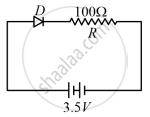
(a) 40 mA
(b) 20 mA
(c) 35 mA
(d) 30 mA - In which of the following figures, the pn diode is reverse biased?
(a)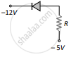
(b)
(c)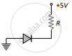
(d)
- Based on the V-I characteristics of the diode, we can classify the diode as:
(a) bilateral device
(b) ohmic device
(c) non-ohmic device
(d) passive element
OR
Two identical PN junctions can be connected in series by three different methods as shown in the figure. If the potential difference in the junctions is the same, then the correct connections will be:
(a) in the circuits (1) and (2)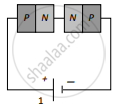

(b) in the circuits (2) and (3)
(c) in the circuits (1) and (3)
(d) only in the circuit (1) 
The V-I characteristic of a diode is shown in the figure. The ratio of the resistance of the diode at I = 15 mA to the resistance at V = -10 V is
(a) 100
(b) 106
(c) 10
(d) 10-6
With reference to a semiconductor diode, define the depletion region.
What is meant by forward biasing of a semiconductor diode?
An ideal PN junction diode offers ______.
A full wave rectifier circuit diodes (D1) and (D2) is shown in the figure. If input supply voltage Vin = 220 sin (100 πt) volt, then at t = 15 ms.

Choose the correct circuit which can achieve the bridge balance.
