Advertisements
Advertisements
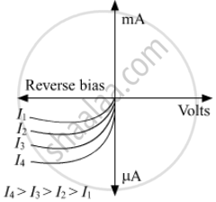
प्रश्न
Draw its I – V characteristics of photodiode
Advertisements
उत्तर
I – V characteristics of photodiode:
APPEARS IN
संबंधित प्रश्न
Plot a graph showing variation of current versus voltage for the material GaAs ?
Show on a graph, the variation of resistivity with temperature for a typical semiconductor.
In semiconductor physics, what is meant by:
(i) rectifier
(ii) an amplifier
(iii) an oscillator
The expected energy of the electron at absolute zero is called:-
On increasing the reverse biases voltage to a large value in a P – N junction diode-current
In the circuit shown in figure, if the diode forward voltage drop is 0.3 V, the voltage difference between A and B is ______.

 (a) |
 (b) |
- Name the type of a diode whose characteristics are shown in figure (A) and figure (B).
- What does the point P in figure (A) represent?
- What does the points P and Q in figure (B) represent?
Answer the following giving reasons:
A p-n junction diode is damaged by a strong current.
Read the following paragraph and answer the questions that follow.
| A semiconductor diode is basically a pn junction with metallic contacts provided at the ends for the application of an external voltage. It is a two-terminal device. When an external voltage is applied across a semiconductor diode such that the p-side is connected to the positive terminal of the battery and the n-side to the negative terminal, it is said to be forward-biased. When an external voltage is applied across the diode such that the n-side is positive and the p-side is negative, it is said to be reverse-biased. An ideal diode is one whose resistance in forward biasing is zero and the resistance is infinite in reverse biasing. When the diode is forward biased, it is found that beyond forward voltage called knee voltage, the conductivity is very high. When the biasing voltage is more than the knee voltage the potential barrier is overcome and the current increases rapidly with an increase in forward voltage. When the diode is reverse biased, the reverse bias voltage produces a very small current of about a few microamperes which almost remains constant with bias. This small current is a reverse saturation current. |
- In the given figure, a diode D is connected to an external resistance R = 100 Ω and an emf of 3.5 V. If the barrier potential developed across the diode is 0.5 V, the current in the circuit will be:
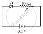
(a) 40 mA
(b) 20 mA
(c) 35 mA
(d) 30 mA - In which of the following figures, the pn diode is reverse biased?
(a)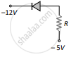
(b)
(c)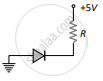
(d)
- Based on the V-I characteristics of the diode, we can classify the diode as:
(a) bilateral device
(b) ohmic device
(c) non-ohmic device
(d) passive element
OR
Two identical PN junctions can be connected in series by three different methods as shown in the figure. If the potential difference in the junctions is the same, then the correct connections will be:
(a) in the circuits (1) and (2)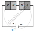

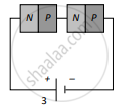
(b) in the circuits (2) and (3)
(c) in the circuits (1) and (3)
(d) only in the circuit (1) 
The V-I characteristic of a diode is shown in the figure. The ratio of the resistance of the diode at I = 15 mA to the resistance at V = -10 V is
(a) 100
(b) 106
(c) 10
(d) 10-6
Draw a labelled characteristic curve (l-V graph) for a semiconductor diode during forward bias.
