Advertisements
Advertisements
Question
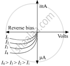
Draw its I – V characteristics of photodiode
Advertisements
Solution
I – V characteristics of photodiode:
APPEARS IN
RELATED QUESTIONS
The plate current in a diode is 20 mA when the plate voltage is 50 V or 60 V. What will be the current if the plate voltage is 70 V?
In semiconductor physics, what is meant by:
(i) rectifier
(ii) an amplifier
(iii) an oscillator
With reference to Semiconductor Physics,
Name the diode that emits spontaneous radiation when forward biased.
In Figure, Vo is the potential barrier across a p-n junction, when no battery is connected across the junction ______.

In the depletion region of a diode ______.
- there are no mobile charges.
- equal number of holes and electrons exist, making the region neutral.
- recombination of holes and electrons has taken place.
- immobile charged ions exist.
Can the potential barrier across a p-n junction be measured by simply connecting a voltmeter across the junction?
Differentiate between the threshold voltage and the breakdown voltage for a diode.
When the p-side and n-side are joined, in which direction do electrons diffuse?
What is the V-I characteristic curve of a diode?
Which expression applies Ohm's law to reverse-biased resistance?
