Advertisements
Advertisements
प्रश्न
When a forward bias is applied to a p-n junction, it ______.
पर्याय
raises the potential barrier.
reduces the majority carrier current to zero.
lowers the potential barrier.
None of the above.
Advertisements
उत्तर
When a forward bias is applied to a p-n junction, it lowers the potential barrier.
Explanation:
When a forward bias is applied to a p-n junction, it lowers the value of potential barrier. In the case of a forward bias, the potential barrier opposes the applied voltage. Hence, the potential barrier across the junction gets reduced.
संबंधित प्रश्न
(i) Explain with the help of a diagram the formation of depletion region and barrier potential in a pn junction.
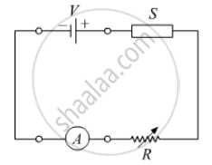
In the following diagram 'S' is a semiconductor. Would you increase or decrease the value of R to keep the reading of the ammeter A constant when S is heated? Give reason for your answer.
What is the use of Zener diode?
Plot a graph showing variation of current versus voltage for the material GaAs ?
Why is a zener diode considered as a special purpose semiconductor diode?
The power delivered in the plate circular of a diode is 1.0 W when the plate voltage is 36 V. Find the power delivered if the plate voltage is increased to 49 V. Assume Langmuir-Child equation to hold.
Find the values of rp, µ and gm of a triode operating at plate voltage 200 V and grid voltage −6. The plate characteristics are shown in the figure.

Answer the following question.
Why photodiodes are required to operate in reverse bias? Explain.
We use alloys for making standard resistors because they have ____________.
With reference to Semiconductor Physics,
Name the diode that emits spontaneous radiation when forward biased.
Of the diodes shown in the following diagrams, which one is reverse biased?
The current through an ideal PN-junction shown in the following circuit diagram will be:

A – pn junction has a depletion layer of thickness .of the order of
Depletion layer in p - n junction diode consists of
The expected energy of the electron at absolute zero is called:-
The breakdown in a reverse biased p–n junction diode is more likely to occur due to ______.
- large velocity of the minority charge carriers if the doping concentration is small.
- large velocity of the minority charge carriers if the doping concentration is large.
- strong electric field in a depletion region if the doping concentration is small.
- strong electric field in the depletion region if the doping concentration is large.
If each diode in figure has a forward bias resistance of 25 Ω and infinite resistance in reverse bias, what will be the values of the current I1, I2, I3 and I4?

The graph of potential barrier versus width of depletion region for an unbiased diode is shown in graph A. In comparison to A, graphs B and C are obtained after biasing the diode in different ways. Identify the type of biasing in B and C and justify your answer
| ‘A’ | ‘B’ | ‘C’ |
 |
 |
 |
Describe the following term briefly:
Minority carrier injection in forward biasing.
