Advertisements
Advertisements
प्रश्न
Explain the formation of the barrier potential in a p-n junction.
Advertisements
उत्तर
A p-n junction is formed by bringing p-type and n-type semiconductors together in very close proximity.
At the instant of p-n-junction, movement of free electrons from the n-side and free holes from the p-side diffuse across the junction and combine and thus leave -ve ions on the p-side and +ve ions inn-side.
These two layers of +ve and -ve ions form the depletion region and the potential difference thus sets up is called the potential barrier.

संबंधित प्रश्न
With the help of neat labelled circuit diagram explain the working of half wave rectifier using semiconductor diode. Draw the input and output waveforms.
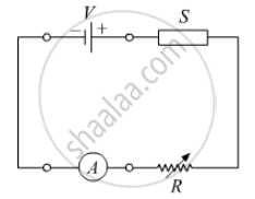
In the following diagram 'S' is a semiconductor. Would you increase or decrease the value of R to keep the reading of the ammeter A constant when S is heated? Give reason for your answer.
Plot a graph showing variation of current versus voltage for the material GaAs ?
Can the potential barrier across a p-n junction be measured by simply connecting a voltmeter across the junction?
A Zener of power rating 1 W is to be used as a voltage regulator. If zener has a breakdown of 5 V and it has to regulate voltage which fluctuated between 3 V and 7 V, what should be the value of Rs for safe operation (Figure)?

Consider a box with three terminals on top of it as shown in figure (a):
 (a) |
Three components namely, two germanium diodes and one resistor are connected across these three terminals in some arrangement. A student performs an experiment in which any two of these three terminals are connected in the circuit shown in figure (b).
 (b) |
The student obtains graphs of current-voltage characteristics for unknown combination of components between the two terminals connected in the circuit. The graphs are
(i) when A is positive and B is negative
 (c) |
(ii) when A is negative and B is positive
 (d) |
(iii) When B is negative and C is positive
|
(e) |

(iv) When B is positive and C is negative
 (f) |
(v) When A is positive and C is negative
 (g) |
(vi) When A is negative and C is positive
 (h) |
From these graphs of current-voltage characteristics shown in figure (c) to (h), determine the arrangement of components between A, B and C.
The graph of potential barrier versus width of depletion region for an unbiased diode is shown in graph A. In comparison to A, graphs B and C are obtained after biasing the diode in different ways. Identify the type of biasing in B and C and justify your answer
| ‘A’ | ‘B’ | ‘C’ |
 |
 |
 |
Differentiate between the threshold voltage and the breakdown voltage for a diode.
Describe the following term briefly:
Minority carrier injection in forward biasing.
With reference to a semiconductor diode, define the potential barrier.
